- 您現(xiàn)在的位置:買賣IC網(wǎng) > PDF目錄352484 > ATTINY2313 (Atmel Corp.) -bit AVR Microcontroller with 8K Bytes In- System Programmable Flash PDF資料下載
參數(shù)資料
| 型號(hào): | ATTINY2313 |
| 廠商: | Atmel Corp. |
| 元件分類: | 8位微控制器 |
| 英文描述: | -bit AVR Microcontroller with 8K Bytes In- System Programmable Flash |
| 中文描述: | 位AVR微控制器具有8K字節(jié)的系統(tǒng)內(nèi)可編程閃存 |
| 文件頁(yè)數(shù): | 51/226頁(yè) |
| 文件大小: | 3676K |
| 代理商: | ATTINY2313 |
第1頁(yè)第2頁(yè)第3頁(yè)第4頁(yè)第5頁(yè)第6頁(yè)第7頁(yè)第8頁(yè)第9頁(yè)第10頁(yè)第11頁(yè)第12頁(yè)第13頁(yè)第14頁(yè)第15頁(yè)第16頁(yè)第17頁(yè)第18頁(yè)第19頁(yè)第20頁(yè)第21頁(yè)第22頁(yè)第23頁(yè)第24頁(yè)第25頁(yè)第26頁(yè)第27頁(yè)第28頁(yè)第29頁(yè)第30頁(yè)第31頁(yè)第32頁(yè)第33頁(yè)第34頁(yè)第35頁(yè)第36頁(yè)第37頁(yè)第38頁(yè)第39頁(yè)第40頁(yè)第41頁(yè)第42頁(yè)第43頁(yè)第44頁(yè)第45頁(yè)第46頁(yè)第47頁(yè)第48頁(yè)第49頁(yè)第50頁(yè)當(dāng)前第51頁(yè)第52頁(yè)第53頁(yè)第54頁(yè)第55頁(yè)第56頁(yè)第57頁(yè)第58頁(yè)第59頁(yè)第60頁(yè)第61頁(yè)第62頁(yè)第63頁(yè)第64頁(yè)第65頁(yè)第66頁(yè)第67頁(yè)第68頁(yè)第69頁(yè)第70頁(yè)第71頁(yè)第72頁(yè)第73頁(yè)第74頁(yè)第75頁(yè)第76頁(yè)第77頁(yè)第78頁(yè)第79頁(yè)第80頁(yè)第81頁(yè)第82頁(yè)第83頁(yè)第84頁(yè)第85頁(yè)第86頁(yè)第87頁(yè)第88頁(yè)第89頁(yè)第90頁(yè)第91頁(yè)第92頁(yè)第93頁(yè)第94頁(yè)第95頁(yè)第96頁(yè)第97頁(yè)第98頁(yè)第99頁(yè)第100頁(yè)第101頁(yè)第102頁(yè)第103頁(yè)第104頁(yè)第105頁(yè)第106頁(yè)第107頁(yè)第108頁(yè)第109頁(yè)第110頁(yè)第111頁(yè)第112頁(yè)第113頁(yè)第114頁(yè)第115頁(yè)第116頁(yè)第117頁(yè)第118頁(yè)第119頁(yè)第120頁(yè)第121頁(yè)第122頁(yè)第123頁(yè)第124頁(yè)第125頁(yè)第126頁(yè)第127頁(yè)第128頁(yè)第129頁(yè)第130頁(yè)第131頁(yè)第132頁(yè)第133頁(yè)第134頁(yè)第135頁(yè)第136頁(yè)第137頁(yè)第138頁(yè)第139頁(yè)第140頁(yè)第141頁(yè)第142頁(yè)第143頁(yè)第144頁(yè)第145頁(yè)第146頁(yè)第147頁(yè)第148頁(yè)第149頁(yè)第150頁(yè)第151頁(yè)第152頁(yè)第153頁(yè)第154頁(yè)第155頁(yè)第156頁(yè)第157頁(yè)第158頁(yè)第159頁(yè)第160頁(yè)第161頁(yè)第162頁(yè)第163頁(yè)第164頁(yè)第165頁(yè)第166頁(yè)第167頁(yè)第168頁(yè)第169頁(yè)第170頁(yè)第171頁(yè)第172頁(yè)第173頁(yè)第174頁(yè)第175頁(yè)第176頁(yè)第177頁(yè)第178頁(yè)第179頁(yè)第180頁(yè)第181頁(yè)第182頁(yè)第183頁(yè)第184頁(yè)第185頁(yè)第186頁(yè)第187頁(yè)第188頁(yè)第189頁(yè)第190頁(yè)第191頁(yè)第192頁(yè)第193頁(yè)第194頁(yè)第195頁(yè)第196頁(yè)第197頁(yè)第198頁(yè)第199頁(yè)第200頁(yè)第201頁(yè)第202頁(yè)第203頁(yè)第204頁(yè)第205頁(yè)第206頁(yè)第207頁(yè)第208頁(yè)第209頁(yè)第210頁(yè)第211頁(yè)第212頁(yè)第213頁(yè)第214頁(yè)第215頁(yè)第216頁(yè)第217頁(yè)第218頁(yè)第219頁(yè)第220頁(yè)第221頁(yè)第222頁(yè)第223頁(yè)第224頁(yè)第225頁(yè)第226頁(yè)
144
2543L–AVR–08/10
ATtiny2313
Start Condition
Detector
The start condition detector is shown in Figure 65. The SDA line is delayed (in the range of 50 to
300 ns) to ensure valid sampling of the SCL line.
The start condition detector is working asynchronously and can therefore wake up the processor
from the Power-down sleep mode. However, the protocol used might have restrictions on the
SCL hold time. Therefore, when using this feature in this case the Oscillator start-up time set by
the CKSEL Fuses (see “Clock Systems and their Distribution” on page 22) must also be taken
into the consideration.
Alternative USI
Usage
When the USI unit is not used for serial communication, it can be set up to do alternative tasks
due to its flexible design.
Half-duplex
Asynchronous Data
Transfer
By utilizing the Shift Register in Three-wire mode, it is possible to implement a more compact
and higher performance UART than by software only.
4-bit Counter
The 4-bit counter can be used as a stand-alone counter with overflow interrupt. Note that if the
counter is clocked externally, both clock edges will generate an increment.
12-bit Timer/Counter
Combining the USI 4-bit counter and Timer/Counter0 allows them to be used as a 12-bit
counter.
Edge Triggered
External Interrupt
By setting the counter to maximum value (F) it can function as an additional external interrupt.
The overflow flag and interrupt enable bit are then used for the external interrupt. This feature is
selected by the USICS1 bit.
Software Interrupt
The counter overflow interrupt can be used as a software interrupt triggered by a clock strobe.
USI Register
Descriptions
USI Data Register –
USIDR
The USI uses no buffering of the serial register, i.e., when accessing the Data Register (USIDR)
the serial register is accessed directly. If a serial clock occurs at the same cycle the register is
written, the register will contain the value written and no shift is performed. A (left) shift operation
is performed depending of the USICS1..0 bits setting. The shift operation can be controlled by
an external clock edge, by a Timer/Counter0 overflow, or directly by software using the USICLK
strobe bit. Note that even when no wire mode is selected (USIWM1..0 = 0) both the external
data input (DI/SDA) and the external clock input (USCK/SCL) can still be used by the Shift
Register.
The output pin in use, DO or SDA depending on the wire mode, is connected via the output latch
to the most significant bit (bit 7) of the Data Register. The output latch is open (transparent) dur-
ing the first half of a serial clock cycle when an external clock source is selected (USICS1 = 1),
and constantly open when an internal clock source is used (USICS1 = 0). The output will be
changed immediately when a new MSB written as long as the latch is open. The latch ensures
that data input is sampled and data output is changed on opposite clock edges.
Note that the corresponding Data Direction Register to the pin must be set to one for enabling
data output from the Shift Register.
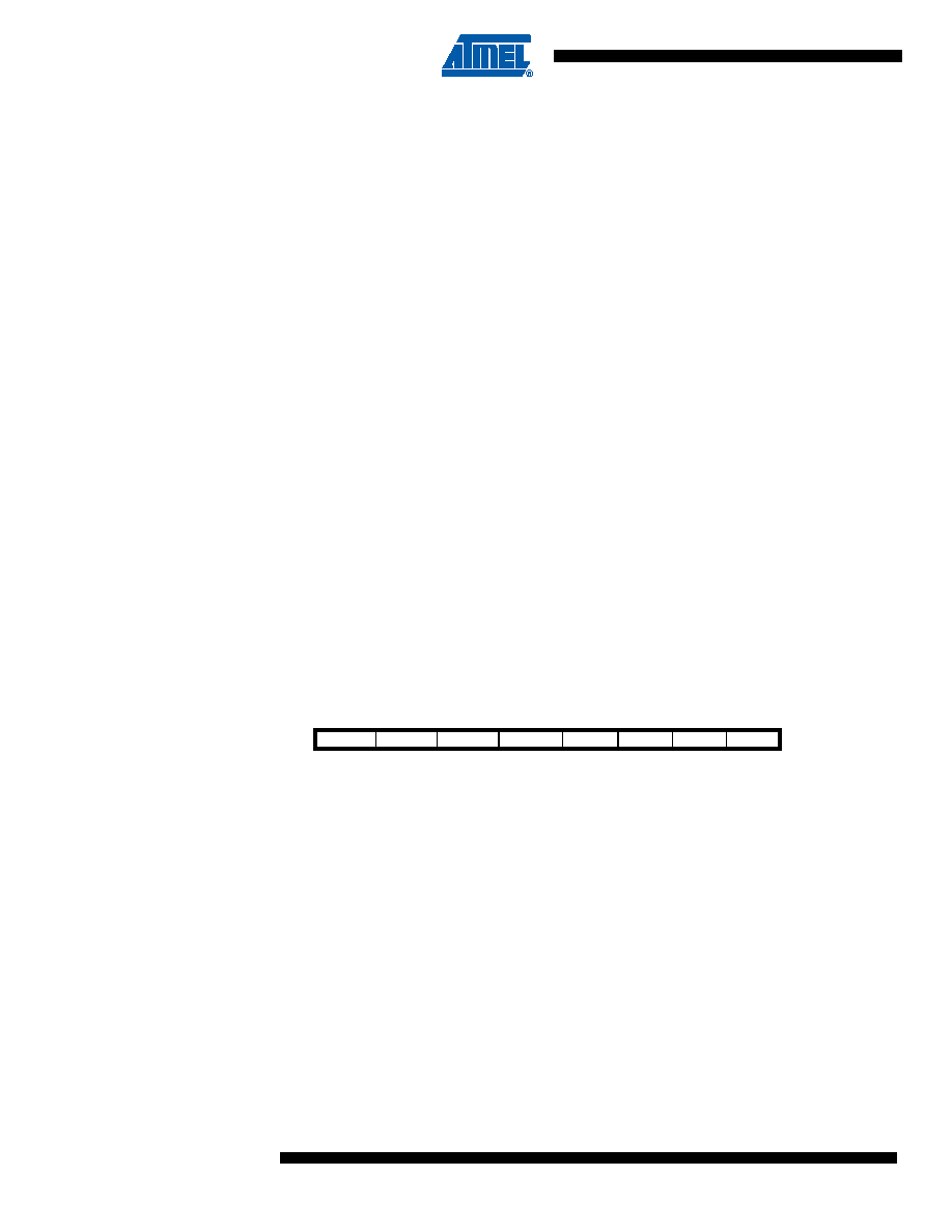
Bit
7
6
5
4
3
2
1
0
MSB
LSB
USIDR
Read/Write
R/W
Initial Value
0
相關(guān)PDF資料 |
PDF描述 |
|---|---|
| ATMEGA128 | -bit AVR Microcontroller with 8K Bytes In- System Programmable Flash |
| AT93C56AU3-10UI-1.8 | 3-wire Serial EEPROMs 2K (256 x 8 or 128 x 16) |
| AT93C56AU3-10UI-2.7 | 3-wire Serial EEPROMs 2K (256 x 8 or 128 x 16) |
| AT93C56AW-10SI-1.8 | 3-wire Serial EEPROMs 2K (256 x 8 or 128 x 16) |
| AT93C56AW-10SI-2.7 | 3-wire Serial EEPROMs 2K (256 x 8 or 128 x 16) |
相關(guān)代理商/技術(shù)參數(shù) |
參數(shù)描述 |
|---|---|
| ATTINY2313_06 | 制造商:ATMEL 制造商全稱:ATMEL Corporation 功能描述:8-bit Microcontroller with 2K Bytes In-System Programmable Flash |
| ATTINY2313-16MI | 制造商:ATMEL 制造商全稱:ATMEL Corporation 功能描述:8-bit AVR Microcontroller with 2K Bytes In-System Programmable Flash |
| ATTINY2313-16MJ | 制造商:ATMEL 制造商全稱:ATMEL Corporation 功能描述:8-bit AVR Microcontroller with 2K Bytes In-System Programmable Flash |
| ATTINY2313-16PI | 制造商:ATMEL 制造商全稱:ATMEL Corporation 功能描述:8-bit AVR Microcontroller with 2K Bytes In-System Programmable Flash |
| ATTINY2313-16PJ | 制造商:ATMEL 制造商全稱:ATMEL Corporation 功能描述:8-bit AVR Microcontroller with 2K Bytes In-System Programmable Flash |
發(fā)布緊急采購(gòu),3分鐘左右您將得到回復(fù)。