- 您現(xiàn)在的位置:買賣IC網 > PDF目錄373026 > BS62XV1024 Automotive Rectifier Diodes PDF資料下載
參數(shù)資料
| 型號: | BS62XV1024 |
| 英文描述: | Automotive Rectifier Diodes |
| 中文描述: | 極低的功率/電壓CMOS SRAM的128K的× 8位(608.41十一) |
| 文件頁數(shù): | 2/30頁 |
| 文件大小: | 608K |
| 代理商: | BS62XV1024 |
第1頁當前第2頁第3頁第4頁第5頁第6頁第7頁第8頁第9頁第10頁第11頁第12頁第13頁第14頁第15頁第16頁第17頁第18頁第19頁第20頁第21頁第22頁第23頁第24頁第25頁第26頁第27頁第28頁第29頁第30頁
2
2-
BSI
Revision 1.0
March 2000
R0201-BS62XV1024
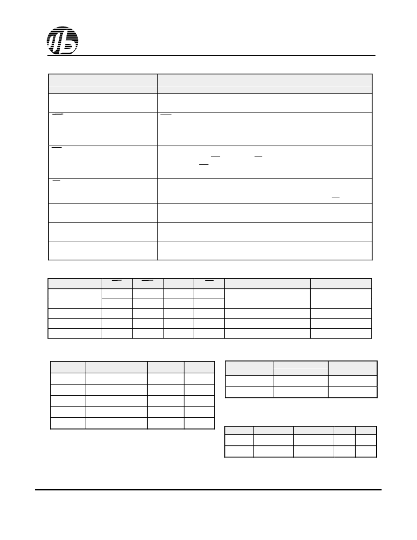
Name
Function
A0-A16 Address Input
These 17 address input select one of the 131,072 x 8-bit words in the RAM
CE1 Chip Enable 1 Input
CE2 Chip Enable 2 Input
CE1 is active LOW and CE2 is active HIGH. Both chip enables must be active to read
from or write to the device. If either chip enable is not active, the device is deselected
and is in a standby power mode. The DQ pins will be in the high impedance state
when the device is deselected.
The write enable input is active LOW and controls read and write operations. With the
chip selected, when WE is HIGH and OE is LOW, output data will be present on the
DQ pins; when WE is LOW, the data present on the DQ pins will be written into the
selected memory location.
The output enable input is active LOW. If the output enable is active while the chip is
selected and the write enable is inactive, data will be present on the DQ pins and they
will be enabled. The DQ pins will be in the high impedance state when OE is inactive.
These 8 bi-directional ports are used to read data from or write data into the RAM.
WE Write Enable Input
OE Output Enable Input
DQ0 – DQ7 Data Input/Output
Ports
Vcc
Power Supply
Gnd
Ground
!
TRUTH TABLE
!
PIN DESCRIPTIONS
MODE
WE
X
X
H
H
L
CE1
H
X
L
L
L
CE2
X
L
H
H
H
OE
X
X
H
L
X
I/O OPERATION
Vcc CURRENT
Not selected
(Power Down)
High Z
I
CCSB
, I
CCSB1
Output Disabled
Read
Write
High Z
D
OUT
D
IN
I
CC
I
CC
I
CC
BS62XV1024
SYMBOL
C
IN
PARAMETER
Input
Capacitance
Input/Output
Capacitance
CONDITIONS
V
IN
=0V
MAX.
6
UNIT
pF
C
DQ
V
I/O
=0V
8
pF
!
ABSOLUTE MAXIMUM RATINGS
(1)
!
OPERATING RANGE
!
CAPACITANCE
(1)
(TA = 25
o
C, f = 1.0 MHz)
1. Stresses greater than those listed under ABSOLUTE MAXIMUM
RATINGS may cause permanent damage to the device. This is a
stress rating only and functional operation of the device at these
or any other conditions above those indicated in the operational
sections of this specification is not implied. Exposure to absolute
maximum rating conditions for extended periods may affect
reliability.
1. This parameter is guaranteed and not tested.
SYMBOL
PARAMETER
Terminal
Respect to GND
RATING
UNITS
V
TERM
Voltage
with
-0.5 to +6.0
V
T
BIAS
Temperature Under Bias
-40 to +125
O
C
T
STG
Storage Temperature
-60 to +150
O
C
P
T
Power Dissipation
1.0
W
I
OUT
DC Output Current
20
mA
RANGE
AMBIENT
TEMPERATURE
0
O
C to +70
O
C
Vcc
Commercial
1.2V ~ 2.4V
Industrial
-40
O
C to +70
O
C
1.2V ~ 2.4V
相關PDF資料 |
PDF描述 |
|---|---|
| BSA21 | Automotive Rectifier Diodes |
| BSFC-SERIES | Automotive Rectifier Diodes |
| BSFZ-SERIES | Automotive Rectifier Diodes |
| BSH102 | N-channel enhancement mode MOS transistor |
| BSH104 | N-channel enhancement mode MOS transistor |
相關代理商/技術參數(shù) |
參數(shù)描述 |
|---|---|
| BS-632-1 | 制造商:PennEngineering (PEM) 功能描述: |
| BS6322 | 制造商:n/a 功能描述:Ships in 2 days |
| BS-632-2 | 制造商:PennEngineering (PEM) 功能描述: |
| BS640GBC3V | 制造商:AMD 制造商全稱:Advanced Micro Devices 功能描述:64 Megabit (4 M x 16-Bit), 1.8 Volt-only Simultaneous Read/Write, Burst Mode Flash Memory |
| BS640GBC4V | 制造商:AMD 制造商全稱:Advanced Micro Devices 功能描述:64 Megabit (4 M x 16-Bit), 1.8 Volt-only Simultaneous Read/Write, Burst Mode Flash Memory |
發(fā)布緊急采購,3分鐘左右您將得到回復。