- 您現(xiàn)在的位置:買賣IC網(wǎng) > PDF目錄366636 > CA3130SX TRANSIL PDF資料下載
參數(shù)資料
| 型號: | CA3130SX |
| 英文描述: | TRANSIL |
| 中文描述: | 電壓反饋運算放大器 |
| 文件頁數(shù): | 7/15頁 |
| 文件大小: | 617K |
| 代理商: | CA3130SX |
2-114
CA3130, CA3130A
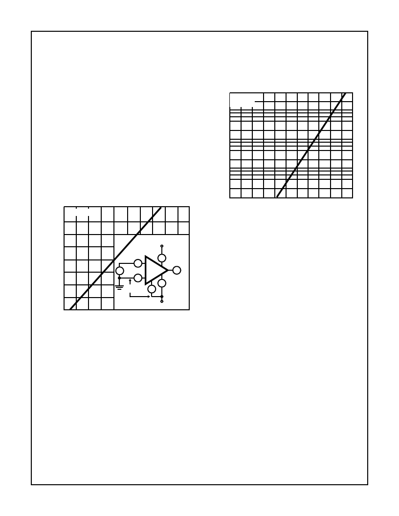
Input Current Variation with Common Mode Input
Voltage
As shown in the Table of Electrical Characteristics, the input
current for the CA3130 Series Op-Amps is typically 5pA at T
A
= +25
o
C when terminals 2 and 3 are at a common-mode
potential of +7.5 volts with respect to negative supply Terminal
4. Figure 10 contains data showing the variation of input cur-
rent as a function of common-mode input voltage at T
A
=
+25
o
C. These data show that circuit designers can advanta-
geously exploit these characteristics to design circuits which
typically require an input current of less than 1pA, provided
the common-mode input voltage does not exceed 2 volts. As
previously noted, the input current is essentially the result of
the leakage current through the gate-protection diodes in the
input circuit and, therefore, a function of the applied voltage.
Although the finite resistance of the glass terminal-to-case
insulator of the TO-5 package also contributes an increment
of leakage current, there are useful compensating factors.
Because the gate-protection network functions as if it is con-
nected to Terminal 4 potential, and the TO-5 case of the
CA3130 is also internally tied to Terminal 4, input terminal 3 is
essentially “guarded” from spurious leakage currents.
FIGURE 10. INPUT CURRENT vs COMMON-MODE VOLTAGE
Offset Nulling
Offset-voltage nulling is usually accomplished with a
100,000-ohm potentiometer connected across Terms. 1 and
5 and with the potentiometer slider arm connected to
Term. 4. A fine offset-null adjustment usually can be effected
with the slider arm positioned in the mid-point of the potenti-
ometer's total range.
Input-Current Variation with Temperature
The input current of the CA3130 Series circuits is typically
5pA at +25
o
C. The major portion of this input current is due
to leakage current through the gate-protective diodes in the
10
7.5
5
2.5
0
-1
0
1
2
3
4
5
6
7
INPUT CURRENT (pA)
I
T
A
= +25
o
C
3
2
7
4
8
6
PA
V
IN
CA3130
15 VOLTS
TO
5 VOLTS
0 VOLTS
TO
-10 VOLTS
V+
V-
input circuit. As with any semiconductor-junction device,
including op-amps with a junction-FET input stage, the leak-
age current approximately doubles for every +10
o
C increase
in temperature. Figure 11 provides data on the typical varia-
tion of input bias current as a function of temperature in the
CA3130.
FIGURE 11. INPUT CURRENT vs AMBIENT TEMPERATURE
In applications requiring the lowest practical input current
and incremental increases in current because of “warm-up”
effects, it is suggested that an appropriate heat sink be used
with the CA3130. In addition, when “sinking” or “sourcing”
significant output current the chip temperature increases,
causing an increase in the input current. In such cases, heat-
sinking can also very markedly reduce and stabilize input
current variations.
Input-Offset-Voltage (V
IO
) Variation with DC Bias vs
Device Operating Life
It is well known that the characteristics of a MOSFET device
can change slightly when a dc gate-source bias potential is
applied to the device for extended time periods. The magni-
tude of the change is increased at high temperatures. Users
of the CA3130 should be alert to the possible impacts of this
effect if the application of the device involves extended oper-
ation at high temperatures with a significant differential dc
bias voltage applied across Terms. 2 and 3. Figure 12 shows
typical data pertinent to shifts in offset voltage encountered
with CA3130 devices (TO-5 package) during life testing. At
lower temperatures (TO-5 and plastic), for example at
+85
o
C, this change in voltage is considerably less. In typical
linear applications where the differential voltage is small and
symmetrical, these incremental changes are of about the
same magnitude as those encountered in an operational
amplifier employing a bipolar transistor input stage. The two-
volt dc differential voltage example represents conditions
when the amplifier output stage is “toggled”, e.g., as in com-
parator applications.
V+ = 7.5V
V- = -7.5V
4000
2
1000
8
6
4
2
100
8
6
4
2
10
8
6
4
2
1
-80
-60
-40
-20
0
20
40
60
80
100 120 140
I
TEMPERATURE (
o
C)
相關PDF資料 |
PDF描述 |
|---|---|
| CA3138 | High-Current, High-Beta N-P-N Transistor Arrays |
| CA3138A | High-Current, High-Beta N-P-N Transistor Arrays |
| CA3160BT | Operational Amplifier |
| CA3094AH | 16A TRIACS |
| CA3094BE | 25 A standard and Snubberless" triacs |
相關代理商/技術參數(shù) |
參數(shù)描述 |
|---|---|
| CA3130T | 制造商:RCA 功能描述: |
| CA3138 | 制造商:GESS 制造商全稱:GESS 功能描述:High-Current, High-Beta N-P-N Transistor Arrays |
| CA3138A | 制造商:GESS 制造商全稱:GESS 功能描述:High-Current, High-Beta N-P-N Transistor Arrays |
| CA3139 | 制造商:未知廠家 制造商全稱:未知廠家 功能描述:電視自動調諧電路 |
| CA3140 | 制造商:INTERSIL 制造商全稱:Intersil Corporation 功能描述:4.5MHz, BiMOS Operational Amplifier with MOSFET Input/Bipolar Output |
發(fā)布緊急采購,3分鐘左右您將得到回復。