- 您現(xiàn)在的位置:買賣IC網(wǎng) > PDF目錄26509 > CS2100P-DZZR (CIRRUS LOGIC INC) PDF資料下載
參數(shù)資料
| 型號: | CS2100P-DZZR |
| 廠商: | CIRRUS LOGIC INC |
| 元件分類: | PLL合成/DDS/VCOs |
| 中文描述: | PHASE LOCKED LOOP, 30 MHz, PDSO10 |
| 封裝: | 3 MM, LEAD FREE, MO-187, MSOP-10 |
| 文件頁數(shù): | 15/25頁 |
| 文件大?。?/td> | 223K |
| 代理商: | CS2100P-DZZR |
Cost Competitive ARCNET (ANSI 878.1) Controller with 2K x 8 On-Chip RAM
SMSC COM20019I
Page 23
Rev. 09-25-07
DATASHEET
Chapter 6
FUNCTIONAL DESCRIPTION
6.1
MICROSEQUENCER
The COM20019I contains an internal microsequencer which performs all of the control operations
necessary to carry out the ARCNET protocol. It consists of a clock generator, a 544 x 8 ROM, a program
counter, two instruction registers, an instruction decoder, a no-op generator, jump logic, and
reconfiguration logic.
The COM20019I derives a 625 kHz and a 312.5 kHz clock from the output clock of the Clock Multiplier.
These clocks provide the rate at which the instructions are executed within the COM20019I. The 625 kHz
clock is the rate at which the program counter operates, while the 312.5 kHz clock is the rate at which the
instructions are executed. The microprogram
is stored in the ROM and the instructions are fetched and then placed into the instruction registers. One
register holds the opcode, while the other holds the immediate data. Once the instruction is fetched, it is
decoded by the internal instruction decoder, at which point the COM20019I proceeds to execute the
instruction. When a no-op instruction is encountered, the microsequencer enters a timed loop and the
program counter is temporarily stopped until the loop is complete. When a jump instruction is encountered,
the program counter is loaded with the jump address from the ROM. The COM20019I contains an internal
reconfiguration timer which interrupts the microsequencer if it has timed out. At this point the program
counter is cleared and the MYRECON bit of the Diagnostic Status Register is set.
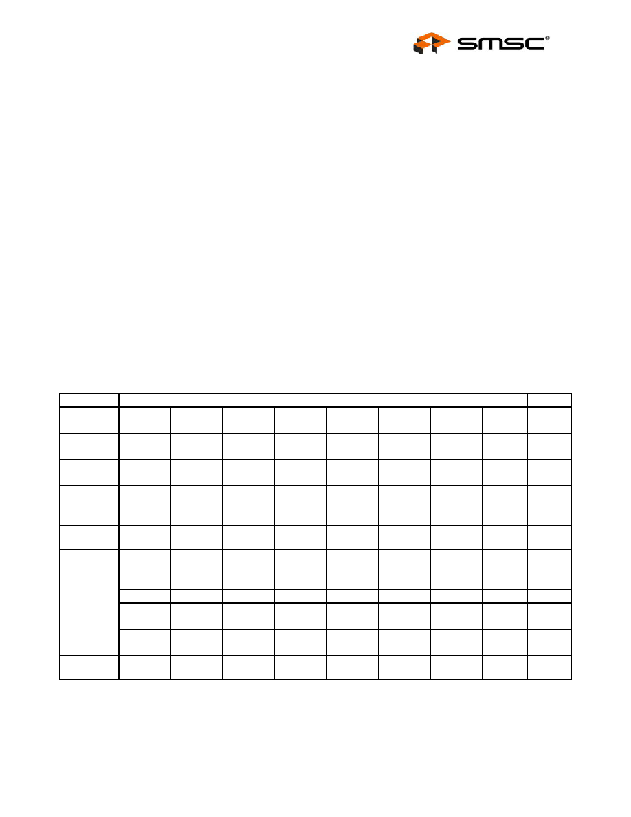
Table 6.1 - Read Register Summary
REGISTER
MSB
READ
LSB
ADDR
STATUS
RI/TRI
X/RI
X/TA
POR
TEST
RECON
TMA
TA/
TTA
00
DIAG.
STATUS
MY-
RECON
DUPID
RCV-
ACT
TOKEN
EXC-
NAK
TENTID
NEW
NEXTID
X
01
ADDRESS
PTR HIGH
RD-
DATA
AUTO-
INC
X
A10
A9
A8
02
ADDRESS
PTR LOW
A7
A6
A5
A4
A3
A2
A1
A0
03
DATA
D7
D6
D5
D4
D3
D2
D1
D0
04
SUB ADR
X
SUB-AD2
SUB-AD1
SUB-
AD0
05
CONFIG-
URATION
RESET
CCHEN
TXEN
ET1
ET2
BACK-
PLANE
SUB-AD1
SUB-
AD0
06
TENTID
TID7
TID6
TID5
TID4
TID3
TID2
TID1
TID0
07-0
NODE ID
NID7
NID6
NID5
NID4
NID3
NID2
NID1
NID0
07-1
SETUP1
P1
MODE
FOUR
NAKS
X
RCV-
ALL
CKP3
CKP2
CKP1
SLOW-
ARB
07-2
NEXT ID
NXT ID7
NXT ID6
NXT ID5
NXT ID4
NXT ID3
NXT
ID2
NXT ID1
NXT
ID0
07-3
SETUP2
RBUS-
TMG
X
EF
NO-
SYNC
RCN-
TM1
RCM-
TM2
07-4
相關(guān)PDF資料 |
PDF描述 |
|---|---|
| CS2200P-DZZR | |
| CS2300P-DZZR | |
| CS3511-CNZR | |
| CS35L00-CNZ | |
| CS4207-DNZR | |
相關(guān)代理商/技術(shù)參數(shù) |
參數(shù)描述 |
|---|---|
| CS2106 | 制造商:Coilcraft Inc 功能描述:NOT RoHS. Current sense transformer (add 'L' for compliant version) |
| CS2106L | 制造商:Coilcraft Inc 功能描述:Current sense transformer, RoHS |
| CS2113-1 | 制造商:Edwards Signaling & Security Systems 功能描述:BELL 432-115V60HZ OTIS |
| CS2113-10 | 制造商:Edwards Signaling & Security Systems 功能描述:GONG |
| CS2113-2 | 制造商:Edwards Signaling & Security Systems 功能描述:BELL 432 115V60AZ OTIS |
發(fā)布緊急采購,3分鐘左右您將得到回復(fù)。