- 您現(xiàn)在的位置:買賣IC網(wǎng) > PDF目錄170345 > CY38050V484-125BBI (CYPRESS SEMICONDUCTOR CORP) LOADABLE PLD, 10 ns, PBGA484 PDF資料下載
參數(shù)資料
| 型號: | CY38050V484-125BBI |
| 廠商: | CYPRESS SEMICONDUCTOR CORP |
| 元件分類: | PLD |
| 英文描述: | LOADABLE PLD, 10 ns, PBGA484 |
| 封裝: | 1 MM PITCH, FBGA-484 |
| 文件頁數(shù): | 43/45頁 |
| 文件大小: | 720K |
| 代理商: | CY38050V484-125BBI |
第1頁第2頁第3頁第4頁第5頁第6頁第7頁第8頁第9頁第10頁第11頁第12頁第13頁第14頁第15頁第16頁第17頁第18頁第19頁第20頁第21頁第22頁第23頁第24頁第25頁第26頁第27頁第28頁第29頁第30頁第31頁第32頁第33頁第34頁第35頁第36頁第37頁第38頁第39頁第40頁第41頁第42頁當前第43頁第44頁第45頁
Quantum38K ISR
CPLD Family
Document #: 38-03043 Rev. *G
Page 7 of 45
Embedded Memory
The Quantum38K architecture includes an embedded channel
memory block at each crossing point of horizontal and vertical
routing channels. The channel memory is a 4096-bit memory
block that can be configured as asynchronous or synchronous
Single-Port RAM, Dual-Port RAM, or Read-Only memory
(ROM). The memory organization is configurable as 4Kx1,
2Kx2, 1Kx4, or 512x8.
Data, address, and control inputs to the channel memory are
driven from horizontal and vertical routing channels. All data
logic outputs drive dedicated tracks in the horizontal and
vertical routing channels. The clocks for the channel memory
block are selected from four global clocks and pin inputs from
the horizontal and vertical channels. The clock muxes also
include a polarity mux for each clock so that the user can
choose an inverted clock.
Dual-Port (Channel Memory) Configuration
Each port has distinct address inputs, as well as separate data
and control inputs that can be accessed simultaneously. The
inputs to the Dual-Port memory are driven from the horizontal
and vertical routing channels. The data outputs drive
dedicated tracks in the routing channels. The interface to the
routing is such that Port A of the Dual-Port interfaces primarily
with the horizontal routing channel and Port B interfaces
primarily with the vertical routing channel.
.
The clocks for each port of the Dual-Port configuration are
selected from four global clocks and two local clocks. One
local clock is sourced from the horizontal channel and the
other from the vertical channel. The data outputs of the
dual-port memory can also be registered. Clocks for the output
registers are also selected from four global clocks and two
local clocks. One clock polarity mux per port allows the use of
true or complement polarity for input and output clocking
purposes.
Arbitration
The Dual-Port configuration of the Channel Memory Block
provides arbitration when both ports access the same address
at the same time. Depending on the memory operations being
attempted, one port always gets priority. See Table 1 for
details on which port gets priority for read and write operations.
An active-LOW ‘Address Match’ signal is generated when an
address collision occurs.
Channel Memory Initialization
The channel memory powers up in an undefined state, but is
set to a user-defined known state during configuration. To facil-
itate the use of look-up-table (LUT) logic and ROM applica-
tions, the channel memory blocks can be initialized with a
given set of data when the device is configured at power up.
For LUT and ROM applications, the user cannot write to
memory blocks.
Channel Memory Routing Interface
Similar to LBC outputs, the channel memory blocks feature
dedicated tracks in the horizontal and vertical routing channels
for the data outputs and the flag outputs, as shown in Figure 5.
This allows the channel memory blocks to be expanded easily.
These dedicated lines can be routed to I/O pins as chip outputs
or to other logic block clusters to be used in logic equations.
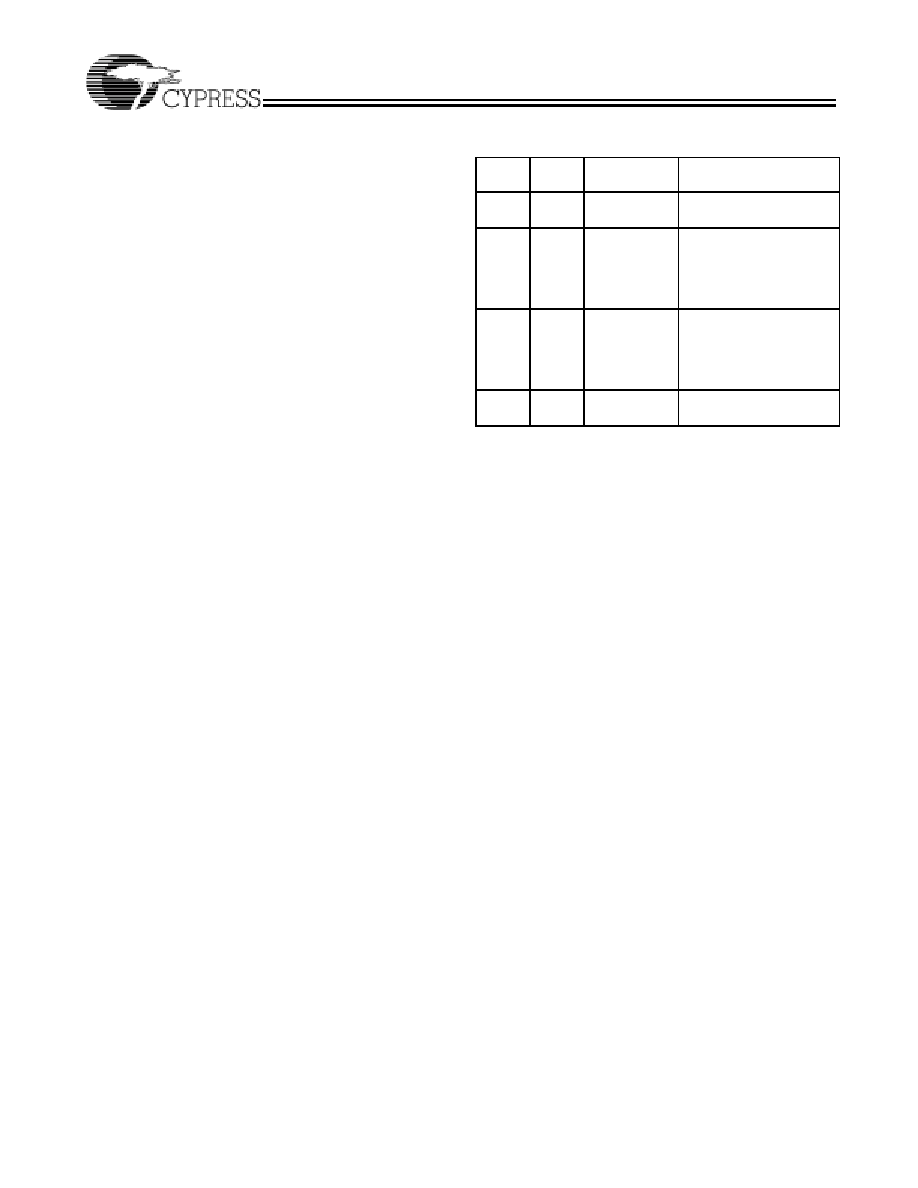
Table 1. Arbitration Result: Address Match Signal
Becomes Active
Port A
Port B
Result of
Arbitration
Comment
Read
No arbitration
required
Both ports read at the
same time
Write
Read
Port A gets
priority
If Port B requests first then
it will read the current
data. The output will then
change to the newly
written data by Port A
Read
Write
Port B gets
priority
If Port A requests first then
it will read the current
data. The output will then
change to the newly
written data by Port B
Write
Port A gets
priority
Port B is blocked until Port
A is finished writing
相關(guān)PDF資料 |
PDF描述 |
|---|---|
| CY39030Z144-222BBC | LOADABLE PLD, 7 ns, PBGA144 |
| CY39030Z144-83BBC | LOADABLE PLD, 15 ns, PBGA144 |
| CY39030Z144-83BBI | LOADABLE PLD, 15 ns, PBGA144 |
| CY39030Z208-222NC | LOADABLE PLD, 7 ns, PQFP208 |
| CY39030Z256-222BBC | LOADABLE PLD, 7 ns, PBGA256 |
相關(guān)代理商/技術(shù)參數(shù) |
參數(shù)描述 |
|---|---|
| CY38100V208-125NTI | 制造商:Cypress Semiconductor 功能描述:CPLD QUANTUM38K 144K GATES 1536 MCRCLLS IND 0.18UM 2.5V/3.3V - Bulk |
| CY3858-000 | 制造商:TE Connectivity 功能描述:2524F0524-1L/9-9-L016 - Cable Rools/Shrink Tubing |
| CY39 | 制造商:PLETRONICS 制造商全稱:Pletronics, Inc. 功能描述:Crystals |
| CY3900I | 功能描述:開發(fā)軟件 ISR Programming Kit RoHS:否 制造商:Atollic Inc. 產(chǎn)品:Compilers/Debuggers 用于:ARM7, ARM9, Cortex-A, Cortex-M, Cortex-R Processors |
| CY3900I_05 | 制造商:CYPRESS 制造商全稱:Cypress Semiconductor 功能描述:Delta39K⑩⁄Ultra37000⑩ ISR⑩ Programming Kits |
發(fā)布緊急采購,3分鐘左右您將得到回復(fù)。