- 您現(xiàn)在的位置:買賣IC網(wǎng) > PDF目錄379056 > CY7C106 (Cypress Semiconductor Corp.) 256K x 4 Static RAM(256K x 4 靜態(tài) RAM) PDF資料下載
參數(shù)資料
| 型號: | CY7C106 |
| 廠商: | Cypress Semiconductor Corp. |
| 英文描述: | 256K x 4 Static RAM(256K x 4 靜態(tài) RAM) |
| 中文描述: | 256K × 4靜態(tài)存儲器(256K × 4靜態(tài)內(nèi)存) |
| 文件頁數(shù): | 4/8頁 |
| 文件大小: | 203K |
| 代理商: | CY7C106 |
CY7C106
CY7C1006
4
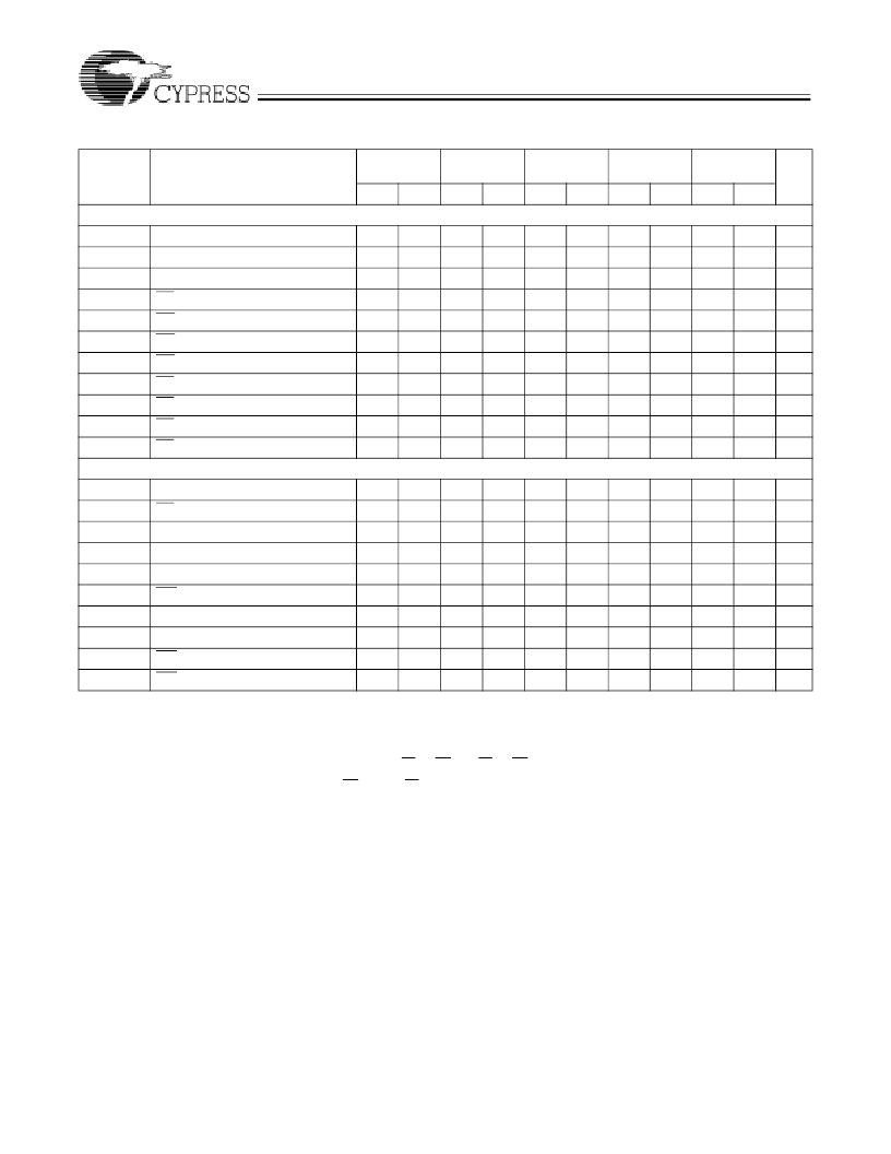
Switching Characteristics
Over the Operating Range
[5]
7C106-12
7C1006-12
Min.
7C106-15
7C1006-15
Min.
7C106-20
7C1006-20
Min.
7C106-25
7C1006-25
Min.
7C106-35
Min.
Parameter
READ CYCLE
t
RC
t
AA
t
OHA
t
ACE
t
DOE
t
LZOE
t
HZOE
t
LZCE
t
HZCE
t
PU
t
PD
WRITE CYCLE
[8,9]
t
WC
t
SCE
t
AW
t
HA
t
SA
t
PWE
t
SD
t
HD
t
LZWE
t
HZWE
Notes:
5.
Test conditions assume signal transition time of 3 ns or less, timing reference levels of 1.5V, input pulse levels of 0 to 3.0V, and output loading of the specified
I
OL
/I
OH
and 30–pF load capacitance.
6.
t
HZOE
, t
HZCE
, and t
HZWE
are specified with a load capacitance of 5 pF as in part (b) of AC Test Loads. Transition is measured
±
500 mV from steady-state voltage.
7.
At any given temperature and voltage condition, t
HZCE
is less than t
LZCE
, t
HZOE
is less than t
LZOE
, and t
HZWE
is less than t
LZWE
for any given device.
8.
The internal write time of the memory is defined by the overlap of CE and WE LOW. CE and WE must be LOW to initiate a write, and the transition of either of these
signals can terminate the write. The input data set-up and hold timing should be referenced to the leading edge of the signal that terminates the write.
9.
The minimum write cycle time for Write Cycle No. 3 (WE controlled, OE LOW) is the sum of t
HZWE
and t
SD
.
Description
Max.
Max.
Max.
Max.
Max.
Unit
Read Cycle Time
Address to Data Valid
Data Hold from Address Change
CE LOW to Data Valid
OE LOW to Data Valid
OE LOW to Low Z
OE HIGH to High Z
[6,7]
CE LOW to Low Z
[7]
CE HIGH to High Z
[6,7]
CE LOW to Power-Up
CE HIGH to Power-Down
12
15
20
25
ns
ns
ns
ns
ns
ns
ns
ns
ns
ns
ns
12
15
20
25
35
3
3
3
3
3
12
6
15
7
20
8
25
10
35
10
0
0
0
0
0
6
7
8
10
10
3
3
3
3
3
6
7
8
10
10
0
0
0
0
0
12
15
20
25
35
Write Cycle Time
CE LOW to Write End
Address Set-Up to Write End
Address Hold from Write End
Address Set-Up to Write Start
WE Pulse Width
Data Set-Up to Write End
Data Hold from Write End
WE HIGH to Low Z
[7]
WE LOW to High Z
[6,7]
12
10
10
0
0
10
7
0
2
15
12
12
0
0
12
8
0
3
20
15
15
0
0
15
10
0
3
25
20
20
0
0
20
15
0
3
35
25
25
0
0
25
20
0
3
ns
ns
ns
ns
ns
ns
ns
ns
ns
ns
6
7
8
10
10
相關(guān)PDF資料 |
PDF描述 |
|---|---|
| CY7C1006 | 256K x 4 Static RAM(256K x4 靜態(tài) RAM) |
| CY7C1146V18 | 18-Mbit DDR-II+ SRAM 2-Word Burst Architecture (2.0 Cycle Read Latency) |
| CY7C1150V18-333BZXC | 18-Mbit DDR-II+ SRAM 2-Word Burst Architecture (2.0 Cycle Read Latency) |
| CY7C1150V18-333BZXI | 18-Mbit DDR-II+ SRAM 2-Word Burst Architecture (2.0 Cycle Read Latency) |
| CY7C1150V18-375BZC | 18-Mbit DDR-II+ SRAM 2-Word Burst Architecture (2.0 Cycle Read Latency) |
相關(guān)代理商/技術(shù)參數(shù) |
參數(shù)描述 |
|---|---|
| CY7C10612DV33-10ZSXI | 功能描述:靜態(tài)隨機(jī)存取存儲器 1024Kbx16 16Mb 3.3V RoHS:否 制造商:Cypress Semiconductor 存儲容量:16 Mbit 組織:1 M x 16 訪問時間:55 ns 電源電壓-最大:3.6 V 電源電壓-最小:2.2 V 最大工作電流:22 uA 最大工作溫度:+ 85 C 最小工作溫度:- 40 C 安裝風(fēng)格:SMD/SMT 封裝 / 箱體:TSOP-48 封裝:Tray |
| CY7C10612DV33-10ZSXIT | 功能描述:靜態(tài)隨機(jī)存取存儲器 1024Kbx16 16Mb 3.3V RoHS:否 制造商:Cypress Semiconductor 存儲容量:16 Mbit 組織:1 M x 16 訪問時間:55 ns 電源電壓-最大:3.6 V 電源電壓-最小:2.2 V 最大工作電流:22 uA 最大工作溫度:+ 85 C 最小工作溫度:- 40 C 安裝風(fēng)格:SMD/SMT 封裝 / 箱體:TSOP-48 封裝:Tray |
| CY7C1061AV33-10BAC | 功能描述:靜態(tài)隨機(jī)存取存儲器 1M x 16 CPG COM Fast Async 靜態(tài)隨機(jī)存取存儲器 RoHS:否 制造商:Cypress Semiconductor 存儲容量:16 Mbit 組織:1 M x 16 訪問時間:55 ns 電源電壓-最大:3.6 V 電源電壓-最小:2.2 V 最大工作電流:22 uA 最大工作溫度:+ 85 C 最小工作溫度:- 40 C 安裝風(fēng)格:SMD/SMT 封裝 / 箱體:TSOP-48 封裝:Tray |
| CY7C1061AV33-10BAI | 制造商:Cypress Semiconductor 功能描述: |
| CY7C1061AV33-10BAXI | 功能描述:靜態(tài)隨機(jī)存取存儲器 16MB (1Mx16) 3.3v 10ns Fast Async 靜態(tài)隨機(jī)存取存儲器 RoHS:否 制造商:Cypress Semiconductor 存儲容量:16 Mbit 組織:1 M x 16 訪問時間:55 ns 電源電壓-最大:3.6 V 電源電壓-最小:2.2 V 最大工作電流:22 uA 最大工作溫度:+ 85 C 最小工作溫度:- 40 C 安裝風(fēng)格:SMD/SMT 封裝 / 箱體:TSOP-48 封裝:Tray |
發(fā)布緊急采購,3分鐘左右您將得到回復(fù)。