- 您現(xiàn)在的位置:買(mǎi)賣IC網(wǎng) > PDF目錄379060 > CY7C1332 (Cypress Semiconductor Corp.) 64K x 18 Synchronous Cache 3.3V RAM(3.3V 64K x 18 同步高速緩沖存儲(chǔ)器 RAM) PDF資料下載
參數(shù)資料
| 型號(hào): | CY7C1332 |
| 廠商: | Cypress Semiconductor Corp. |
| 英文描述: | 64K x 18 Synchronous Cache 3.3V RAM(3.3V 64K x 18 同步高速緩沖存儲(chǔ)器 RAM) |
| 中文描述: | 64K的× 18同步高速緩存3.3V的內(nèi)存電壓(3.3V 64K的× 18同步高速緩沖存儲(chǔ)器的RAM) |
| 文件頁(yè)數(shù): | 1/13頁(yè) |
| 文件大小: | 313K |
| 代理商: | CY7C1332 |
當(dāng)前第1頁(yè)第2頁(yè)第3頁(yè)第4頁(yè)第5頁(yè)第6頁(yè)第7頁(yè)第8頁(yè)第9頁(yè)第10頁(yè)第11頁(yè)第12頁(yè)第13頁(yè)
ADVANCED INFORMATION
64K x 18 Synchronous
Cache 3.3V RAM
Functional Description
The CY7C1331 and CY7C1332 are 3.3V 64K by 18 synchro-
nous cache RAMs designed to interface with high-speed mi-
croprocessors with minimum glue logic. Maximum access de-
lay from clock rise is 8.5 ns. A 2-bit on-chip counter captures
the first address in a burst and increments the address auto-
matically for the rest of the burst access.
The CY7C1331 is designed for Intel Pentium and i486
CPU-based systems; its counter follows the burst sequence of
the Pentium and the i486 processors. The CY7C1332 is archi-
tected for processors with linear burst sequences. Burst ac-
cesses can be initiated with the processor address strobe (AD-
SP) or the cache controller address strobe (ADSC) inputs.
Address advancement is controlled by the address advance-
ment (ADV) input.
A synchronous self-timed write mechanism is provided to sim-
plify the write interface. A synchronous chip select input and
an asynchronous output enable input provide easy control for
bank selection and output three-state control.
CY7C1331
CY7C1332
Cypress Semiconductor Corporation
3901 North First Street
San Jose
CA 95134
December 1992 - Revised April 1995
408-943-2600
Features
Supports 66-MHz Pentium processor cache systems
with zero wait states
Single 3.3V power supply
64K by 18 common I/O
Fast clock-to-output times
—8.5 ns
Two-bit wraparound counter supporting the Pentium
and 486 burst sequence (7C1331)
Two-bit wraparound counter supporting linear burst se-
quence (7C1332)
Separate processor and controller address strobes
Synchronous self-timed write
Direct interface with the processor and external cache
controller
Asynchronous output enable
JEDEC-standard pinout
52-pin PLCC and PQFP packaging
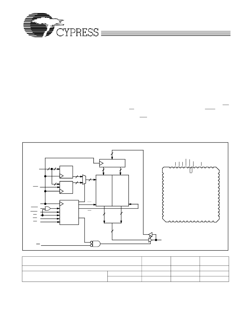
LogicBlockDiagram
Pin Configuration
1331–1
Top View
PLCC
1331– 2
18
16
14
14
2
2
16
9
9
9
9
18
ADV
CLK
TIMING
CONTROL
REG
ADV
LOGIC
REGISTER
64K X 9
RAM ARRAY
64K X 9
RAM ARRAY
OE
1
7C1331
7C1332
8
9
10
11
12
13
14
15
16
17
18
19
20
46
45
44
43
42
41
40
39
38
37
36
35
34
2122 23 24 25 26 27 28 29 30 31 32 33
7 6 5 4 3 2
52 51 50 49 48 47
A
5
A
4
A
3
A
2
C
V
A
A
A
A
A
A
1
G
A
6
C
C
A
DQ
8
DQ
9
V
CCQ
V
SSQ
DQ
10
DQ
11
DQ
12
DQ
13
V
SSQ
V
CCQ
DQ
14
DQ
15
DP1
[2]
A
9
A
7
DP
0
DQ
7
DQ
6
V
CCQ
V
SSQ
DQ
5
DQ
4
DQ
3
DQ
2
V
SSQ
V
CCQ
DQ
1
DQ
0
[2]
A
O
A
A
A
W
W
A
15
– A
0
DATA
IN
ADSP
ADSC
CS
WH
WL
WH
WL
DQ
15
– DQ
0
DP
1
– DP
0
A
8
1
1
1
1
1
1
Selection Guide
7C1331–8
7C1332–8
8.5
200
7C1331–10
7C1332–10
10
200
7C1331–12
7C1332–12
12
170
200
Maximum Access Time (ns)
Maximum Operating Current (mA)
Commercial
Military
Notes:
1.
Pentium is a trademark of Intel Corporation.
DP
and DP
are functionally equivalent to DQ
x
.
相關(guān)PDF資料 |
PDF描述 |
|---|---|
| CY7C1331 | 64K x 18 Synchronous Cache 3.3V RAM(3.3V 64K x 18 同步高速緩沖存儲(chǔ)器 RAM) |
| CY7C1333 | 64Kx32 Flow-Thru SRAM with NoBL Architecture(帶NoBL結(jié)構(gòu)的64Kx32流通式 SRAM) |
| CY7C1334 | 64Kx32 Flow-Thru SRAM with NoBL Architecture(帶NoBL結(jié)構(gòu)的64Kx32流通式 SRAM) |
| CY7C1335 | 32K x 32 Synchronous-Pipelined Cache RAM(32K x 32 同步流水線式高速緩沖存儲(chǔ)器 RAM) |
| CY7C1336 | 64K x 32 Synchronous Flow-Through 3.3V Cache RAM(3.3V 64K x 32 同步流通式高速緩沖RAM) |
相關(guān)代理商/技術(shù)參數(shù) |
參數(shù)描述 |
|---|---|
| CY7C133-25JC | 制造商:Cypress Semiconductor 功能描述:Static RAM, 2Kx16, 68 Pin, Plastic, LDCC |
| CY7C1332AV25-200BGC | 制造商:Cypress Semiconductor 功能描述: |
| CY7C1333-50AC | 制造商:Rochester Electronics LLC 功能描述:- Bulk |
| CY7C133-35JC | 制造商:Cypress Semiconductor 功能描述:SRAM Chip Async Dual 5V 32K-Bit 2K x 16 35ns 68-Pin PLCC |
| CY7C1333-66AC | 制造商:Rochester Electronics LLC 功能描述:- Bulk |
發(fā)布緊急采購(gòu),3分鐘左右您將得到回復(fù)。