- 您現(xiàn)在的位置:買賣IC網(wǎng) > PDF目錄379060 > CY7C1334 (Cypress Semiconductor Corp.) 64Kx32 Flow-Thru SRAM with NoBL Architecture(帶NoBL結(jié)構(gòu)的64Kx32流通式 SRAM) PDF資料下載
參數(shù)資料
| 型號(hào): | CY7C1334 |
| 廠商: | Cypress Semiconductor Corp. |
| 英文描述: | 64Kx32 Flow-Thru SRAM with NoBL Architecture(帶NoBL結(jié)構(gòu)的64Kx32流通式 SRAM) |
| 中文描述: | 64Kx32流過式的SRAM架構(gòu)的總線延遲(帶總線延遲結(jié)構(gòu)的64Kx32流通式的SRAM) |
| 文件頁數(shù): | 5/11頁 |
| 文件大?。?/td> | 184K |
| 代理商: | CY7C1334 |
CY7C1334
5
Burst Write Accesses
The CY7C1334 has an on-chip burst counter that allows the
user the ability to supply a single address and conduct up to
four Write operations without reasserting the address inputs.
ADV/LD must be driven LOW in order to load the initial ad-
dress, as described in the Single Write Access section above.
When ADV/LD is driven HIGH on the subsequent clock rise,
the chip enables (CE
1
, CE
2
, and CE
3
) and WE inputs are ig-
nored and the burst counter is incremented. The correct
BWS
[3:0]
inputs must be driven in each cycle of the burst write
in order to write the correct bytes of data.
Notes:
1.
X=
”
Don't Care
”
, 1=Logic HIGH, 0=Logic LOW, CE stands for ALL Chip Enables active.BWS
= 0 signifies at least one Byte Write Select is active, BWS
x
= Valid
signifies that the desired byte write selects are asserted, see Write Cycle Description table for details.
Write is defined by WE and BWS
. See Write Cycle Description table for details.
The DQ pins are controlled by the current cycle and the OE signal.
CEN=1 inserts wait states.
CEN=1 inserts wait states.
Device will power-up deselected and the I/Os in a three-state condition, regardless of OE.
OE assumed LOW.
2.
3.
4.
5.
6.
7.
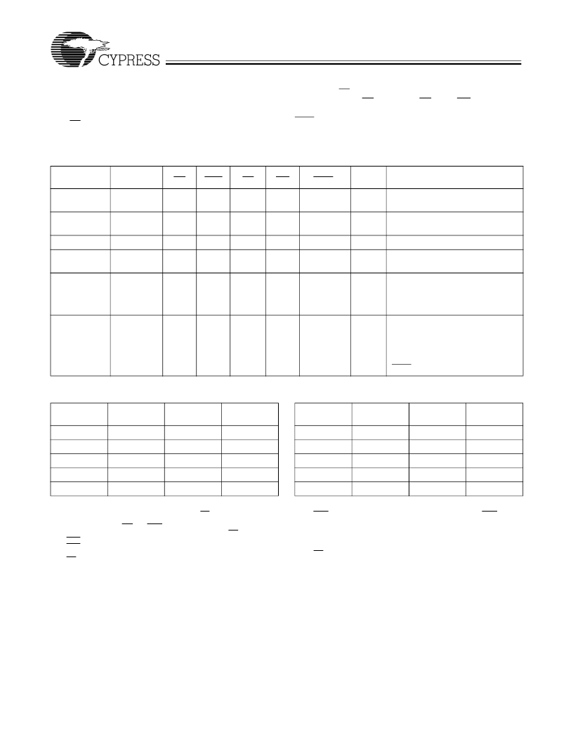
Cycle Description Truth Table
[1, 2, 3, 4, 6, 7]
Operation
Address
Used
CE
CEN
ADV/
LD
WE
BWS
x
X
CLK
Comments
Deselected
External
1
0
L
X
L-H
I/Os three-state following next rec-
ognized clock.
Suspend
-
X
1
X
X
X
L-H
Clock ignored, all operations sus-
pended.
Begin Read
External
0
0
0
1
X
L-H
Address latched.
Begin Write
External
0
0
0
0
Valid
L-H
Address latched, data presented
two valid clocks later.
Burst Read
Operation
Internal
X
0
1
X
X
L-H
Burst Read operation. Previous
access was a Read operation. Ad-
dresses incremented internally in
conjunction with the state of Mode.
Burst Write
Operation
Internal
X
0
1
X
Valid
L-H
Burst Write operation. Previous
access was a Write operation. Ad-
dresses incremented internally in
conjunction with the state of Mode.
Bytes written are determined by
BWS
[3:0]
.
Interleaved Burst Sequence
First
Address
Ax+1, Ax
Second
Address
Ax+1, Ax
Third
Address
Ax+1, Ax
Fourth
Address
Ax+1, Ax
00
01
10
11
01
00
11
10
10
11
00
01
11
10
01
00
Linear Burst Sequence
First
Address
Ax+1, Ax
Second
Address
Ax+1, Ax
Third
Address
Ax+1, Ax
Fourth
Address
Ax+1, Ax
00
01
10
11
01
10
11
00
10
11
00
01
11
00
01
10
相關(guān)PDF資料 |
PDF描述 |
|---|---|
| CY7C1335 | 32K x 32 Synchronous-Pipelined Cache RAM(32K x 32 同步流水線式高速緩沖存儲(chǔ)器 RAM) |
| CY7C1336 | 64K x 32 Synchronous Flow-Through 3.3V Cache RAM(3.3V 64K x 32 同步流通式高速緩沖RAM) |
| CY7C1337 | 32K x 32 Synchronous-Pipelined Cache RAM(32K x 32 同步流水線式高速緩沖存儲(chǔ)器 RAM) |
| CY7C1338G-117AXI | 4-Mbit (128K x 32) Flow-Through Sync SRAM |
| CY7C1338G-133BGXI | 4-Mbit (128K x 32) Flow-Through Sync SRAM |
相關(guān)代理商/技術(shù)參數(shù) |
參數(shù)描述 |
|---|---|
| CY7C1334-50AC | 制造商:Rochester Electronics LLC 功能描述:- Bulk |
| CY7C1334-50ACT | 制造商:Rochester Electronics LLC 功能描述:- Bulk |
| CY7C1334-80AC | 制造商:Rochester Electronics LLC 功能描述:- Bulk |
| CY7C1334H-166AXC | 功能描述:靜態(tài)隨機(jī)存取存儲(chǔ)器 64Kx32 3.3V NoBL Sync PL 靜態(tài)隨機(jī)存取存儲(chǔ)器 RoHS:否 制造商:Cypress Semiconductor 存儲(chǔ)容量:16 Mbit 組織:1 M x 16 訪問時(shí)間:55 ns 電源電壓-最大:3.6 V 電源電壓-最小:2.2 V 最大工作電流:22 uA 最大工作溫度:+ 85 C 最小工作溫度:- 40 C 安裝風(fēng)格:SMD/SMT 封裝 / 箱體:TSOP-48 封裝:Tray |
| CY7C133-55JC | 制造商:Cypress Semiconductor 功能描述:SRAM Chip Async Dual 5V 32K-Bit 2K x 16 55ns 68-Pin PLCC |
發(fā)布緊急采購,3分鐘左右您將得到回復(fù)。