- 您現(xiàn)在的位置:買賣IC網(wǎng) > PDF目錄379097 > CY8C20234 (Cypress Semiconductor Corp.) PSoC Mixed-Signal Array(PSoC混合信號陣列) PDF資料下載
參數(shù)資料
| 型號: | CY8C20234 |
| 廠商: | Cypress Semiconductor Corp. |
| 英文描述: | PSoC Mixed-Signal Array(PSoC混合信號陣列) |
| 中文描述: | PSoC混合信號陣列(的PSoC混合信號陣列) |
| 文件頁數(shù): | 10/32頁 |
| 文件大小: | 378K |
| 代理商: | CY8C20234 |
第1頁第2頁第3頁第4頁第5頁第6頁第7頁第8頁第9頁當(dāng)前第10頁第11頁第12頁第13頁第14頁第15頁第16頁第17頁第18頁第19頁第20頁第21頁第22頁第23頁第24頁第25頁第26頁第27頁第28頁第29頁第30頁第31頁第32頁
September 18, 2006
Document No. 001-05356 Rev. *B
10
CY8C20234, CY8C20334, CY8C20434 Final Data Sheet
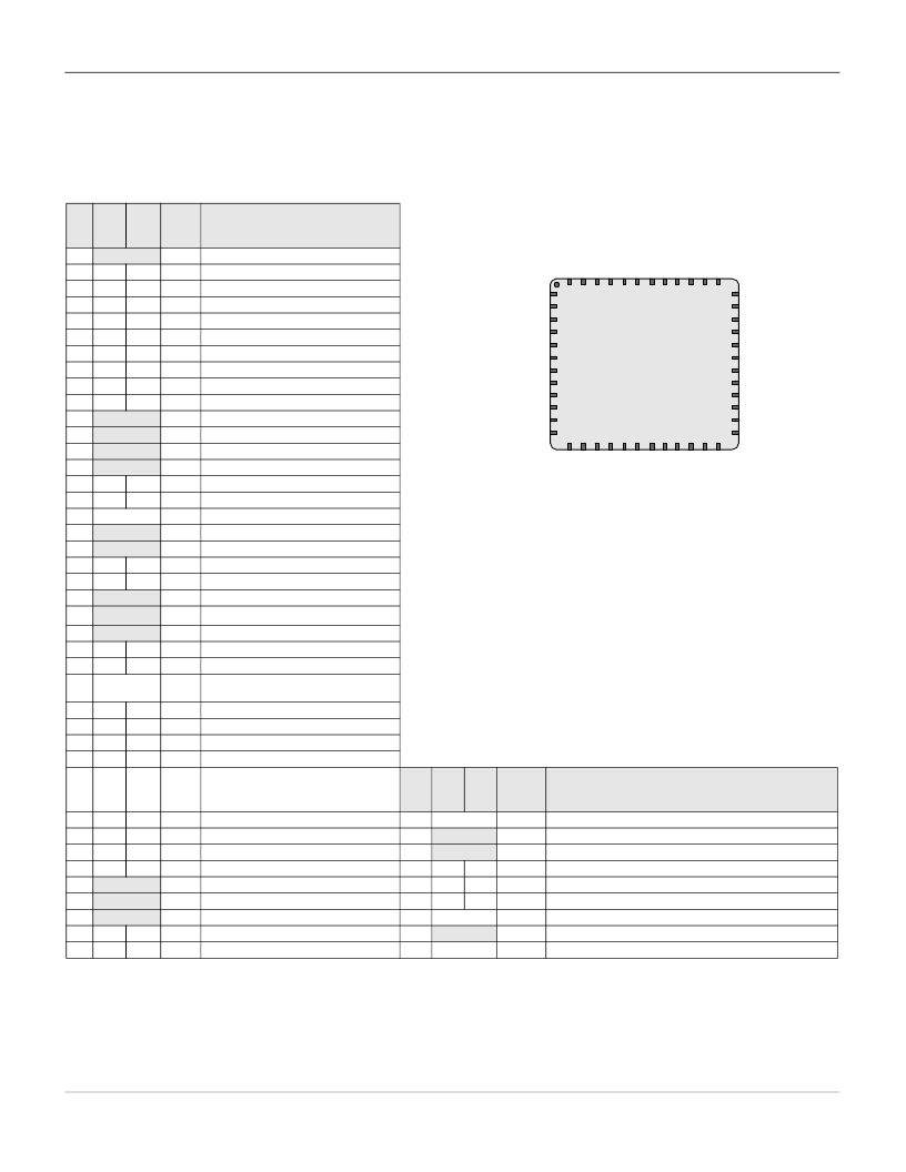
1. Pin Information
1.1.4
48-Pin OCD Part Pinout
The 48-pin QFN part table and drawing below is for the CY8C20000 On-Chip Debug (OCD) PSoC device.
Note
This part is only used for in-circuit debugging. It is NOT available for production
Table 1-4. 48-Pin OCD Part Pinout (QFN**)
Pin
No.
D
A
Name
Description
CY8C20000 OCD PSoC Device
1
2
3
4
5
6
7
8
9
10
11
12
13
14
15
16
17
18
19
20
21
22
23
NC
P0[1]
P2[7]
P2[5]
P2[3]
P2[1]
P3[3]
P3[1]
P1[7]
P1[5]
NC
NC
NC
NC
P1[3]
P1[1]
Vss
CCLK
HCLK
P1[0]
P1[2]
NC
NC
No connection.
IO
IO
IO
IO
IO
IO
IO
IOH
IOH
I
I
I
I
I
I
I
I
I
I2C SCL, SPI SS.
I2C SDA, SPI MISO.
No connection.
No connection.
No connection.
No connection.
SPI CLK.
CLK*, I2C SCL, SPI MOSI.
Ground connection.
OCD CPU clock output.
OCD high speed clock output.
DATA*, I2C SDA.
IOH
IOH
I
I
Power
IOH
IOH
I
I
No connection.
No connection.
Not for Production
24
25
26
27
NC
P1[4]
P1[6]
XRES
No connection.
Optional external clock input (EXTCLK).
IOH
IOH
I
I
Input
Active high external reset with internal
pull down.
28
29
30
31
32
IO
IO
IO
IO
IO
I
I
I
I
I
P3[0]
P3[2]
P2[0]
P2[2]
P2[4]
Pin
No.
D
A
Name
Description
33
34
35
36
37
38
39
40
IO
IO
IO
IO
I
I
I
I
P2[6]
P0[0]
P0[2]
P0[4]
NC
NC
NC
P0[6]
41
42
43
44
45
46
47
48
CP
Power
Vdd
OCDO
OCDE
P0[7]
P0[5]
P0[3]
Vss
NC
Vss
Supply voltage.
OCD even data IO.
OCD odd data output.
IO
IO
IO
I
I
I
No connection.
No connection.
No connection.
Analog bypass.
Integrating input.
Ground connection.
No connection.
Center pad must be connected to ground.
Power
IO
I
Power
LEGEND
A = Analog, I = Input, O = Output, NC = No Connection H = 5 mA High Output Drive.
* ISSP pin which is not HighZ at POR. See the
PSoC Mixed-Signal Array Technical Reference Manual
for details.
** The center pad on the QFN package should be connected to ground (Vss) for best mechanical, thermal, and electrical performance. If not connected to ground, it
should be electrically floated and not connected to any other signal.
OCD QFN
(Top View)
N
V
P
P
P
O
O
V
P
N
N
N
10
11
12
NC
AI, P0[1]
AI, P2[7]
AI, P2[5]
AI, P2[3]
AI, P2[1]
AI, P3[3]
AI, P3[1]
AI, I2C SCL, SPI SS, P1[7]
AI, I2C SDA, SPI MISO, P1[5]
NC
NC
35
34
33
32
31
30
29
28
27
26
25
36
4
1
2
3
4
5
6
7
8
9
4
4
4
4
4
4
4
4
3
3
3
P0[2], AI
P0[0], AI
P2[6], AI
P2[4], AI
P2[2], AI
P2[0], AI
P3[2], AI
P3[0], AI
XRES
P1[6], AI
P1[4], EXTCLK, AI
P0[4], AI
1
1
1
1
1
1
1
2
2
2
2
2
N
N
A
A
V
C
H
A
A
N
N
N
相關(guān)PDF資料 |
PDF描述 |
|---|---|
| CY8C20334 | PSoC Mixed-Signal Array(PSoC混合信號陣列) |
| CY8C22213-24PVIT | PSoC Mixed Signal Array |
| CY8C22113 | PSoC Mixed Signal Array |
| CY8C22113-24PI | PSoC Mixed Signal Array |
| CY8C22113-24SI | PSoC Mixed Signal Array |
相關(guān)代理商/技術(shù)參數(shù) |
參數(shù)描述 |
|---|---|
| CY8C20234_09 | 制造商:CYPRESS 制造商全稱:Cypress Semiconductor 功能描述:PSoC Programmable System-0n-Chip |
| CY8C20234_10 | 制造商:CYPRESS 制造商全稱:Cypress Semiconductor 功能描述:Automotive PSoC? Programmable System-on-Chip |
| CY8C20234_11 | 制造商:CYPRESS 制造商全稱:Cypress Semiconductor 功能描述:Automotive PSoC Programmable System-on-Chip |
| CY8C20234-12LKXA | 功能描述:可編程片上系統(tǒng) - PSoC 13 I/O 8K FLASH 512 SRAM RoHS:否 制造商:Cypress Semiconductor 核心:8051 處理器系列:CY8C36 數(shù)據(jù)總線寬度:8 bit 最大時鐘頻率:67 MHz 程序存儲器大小:32 KB 數(shù)據(jù) RAM 大小:4 KB 片上 ADC:Yes 工作電源電壓:0.5 V to 5.5 V 工作溫度范圍:- 40 C to + 85 C 封裝 / 箱體:QFN-68 安裝風(fēng)格:SMD/SMT |
| CY8C20234-12LKXAT | 功能描述:可編程片上系統(tǒng) - PSoC 13 I/O 8K FLASH 512 SRAM RoHS:否 制造商:Cypress Semiconductor 核心:8051 處理器系列:CY8C36 數(shù)據(jù)總線寬度:8 bit 最大時鐘頻率:67 MHz 程序存儲器大小:32 KB 數(shù)據(jù) RAM 大小:4 KB 片上 ADC:Yes 工作電源電壓:0.5 V to 5.5 V 工作溫度范圍:- 40 C to + 85 C 封裝 / 箱體:QFN-68 安裝風(fēng)格:SMD/SMT |
發(fā)布緊急采購,3分鐘左右您將得到回復(fù)。