- 您現(xiàn)在的位置:買賣IC網(wǎng) > PDF目錄376836 > DP84422BN DRAM Controller PDF資料下載
參數(shù)資料
| 型號(hào): | DP84422BN |
| 英文描述: | DRAM Controller |
| 中文描述: | DRAM控制器 |
| 文件頁數(shù): | 8/46頁 |
| 文件大?。?/td> | 644K |
| 代理商: | DP84422BN |
第1頁第2頁第3頁第4頁第5頁第6頁第7頁當(dāng)前第8頁第9頁第10頁第11頁第12頁第13頁第14頁第15頁第16頁第17頁第18頁第19頁第20頁第21頁第22頁第23頁第24頁第25頁第26頁第27頁第28頁第29頁第30頁第31頁第32頁第33頁第34頁第35頁第36頁第37頁第38頁第39頁第40頁第41頁第42頁第43頁第44頁第45頁第46頁

3.0 Signal Descriptions
(Continued)
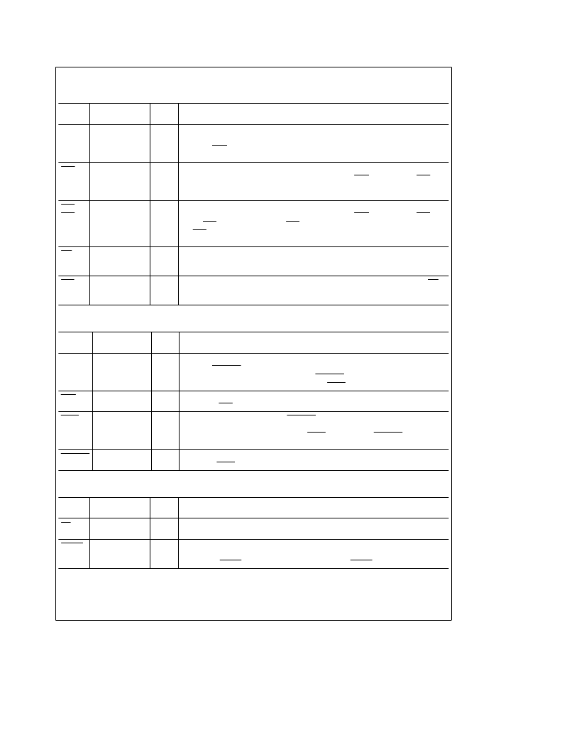
3.2 DRAM CONTROL SIGNALS
Pin
Name
Device (if not
Applicable to All)
Input/
Output
Description
Q0–11
Q0–12
DP8440
DP8441
O
DRAM ADDRESS:
These output signals are the multiplexed outputs of the R0–11/12 and
C0–11/12 and form the DRAM address bus. These outputs contain the refresh address
whenever RFIP is asserted. They have high capacitive drivers with 20
X
s series damping
resistors.
RAS0–3
O
ROW ADDRESS STROBES:
These outputs are asserted to latch the row address
contained on the outputs Q0–11/12 into the DRAM. When RFIP is asserted, the RAS
outputs are used to latch the refresh row address contained on the Q0–11/12 outputs into
the DRAM. These outputs have high capacitive drivers with 20
X
series damping resistors.
CAS0–3
CAS0–7
DP8440
DP8441
O
COLUMN ADDRESS STROBES:
These outputs are asserted to latch the column address
contained on the outputs Q0–11/12 into the DRAM. When RFIP is asserted and CAS-
before-RAS refresh is selected, the CAS outputs will assert 1T (one clock period) before
the RAS outputs are asserted. These outputs have high capacitive drivers with 20
X
series
damping resistors.
WE
O
WRITE ENABLE:
This output asserted specifies a write operation to the DRAM. When
negated, this output specifies a read operation to the DRAM. This output has a high
capacitive driver and a 20
X
series damping resistor.
WIN
I
WRITE ENABLE IN:
This input is used to signify a write operation to the DRAM. The WE
output will follow this input. Also, this input controls the precharge time for Read and Write
during Burst Mode Access.
3.3 REFRESH SIGNALS
Pin
Name
Device (if not
Applicable to All) Output
Input/
Description
RFRQ
O
REFRESH REQUEST:
When RFRQ is asserted, it specifies that 15
m
s or 120
m
s have
passed. If DISRFSH is negated and the controller is not into an access cycle, the
DP8440/41 will perform an internal refresh. If DISRFSH is asserted, RFRQ can be used to
externally request a refresh by asserting the input RFSH.
RFIP
O
REFRESH IN PROGRESS:
This output is asserted prior to a refresh cycle and is negated
when all the RAS outputs are negated for that refresh.
RFSH
I
REFRESH:
This input asserted with DISRFSH already asserted will request a refresh. If
this input is continually asserted, the DP8440/41 will perform refresh cycles in a burst
refresh fashion until the input is negated. If RFSH is asserted with DISRFSH negated, the
internal refresh address counter is cleared. This technique is useful for burst refreshes.
DISRFSH
I
DISABLE REFRESH:
This input is used to disable internal refreshes and must be asserted
when using RFSH for externally requested refreshes.
3.4 RESET AND PROGRAMMING SIGNALS
Pin
Name
Device (if not
Applicable to All)
Input/
Output
Description
ML
I
MODE LOAD:
This input signal, when low, enables the internal programming register that
stores the programming information.
RESET
I
SYSTEM RESET:
Reset forces the DP8440/41 to be set at a known state. V
CC
, CLK and
DELCLK have to reach their proper DC and AC specifications for at least 1 ms before
negating the RESET signal. All outputs are negated when RESET is asserted.
8
相關(guān)PDF資料 |
PDF描述 |
|---|---|
| DP84422J | DRAM Controller |
| DP84422N | DRAM Controller |
| DP84432J | DRAM Controller |
| DP84432N | DRAM Controller |
| DP8472 | Floppy Disk Controller |
相關(guān)代理商/技術(shù)參數(shù) |
參數(shù)描述 |
|---|---|
| DP84422J | 制造商:未知廠家 制造商全稱:未知廠家 功能描述:DRAM Controller |
| DP84422J/A+ | 制造商:未知廠家 制造商全稱:未知廠家 功能描述:DRAM Controller |
| DP84422N | 制造商:未知廠家 制造商全稱:未知廠家 功能描述:DRAM Controller |
| DP84422N/A+ | 制造商:未知廠家 制造商全稱:未知廠家 功能描述:DRAM Controller |
| DP84422N/B+ | 制造商:未知廠家 制造商全稱:未知廠家 功能描述:DRAM Controller |
發(fā)布緊急采購,3分鐘左右您將得到回復(fù)。