- 您現(xiàn)在的位置:買賣IC網(wǎng) > PDF目錄295864 > E0C88F360F 8-BIT, MROM, 8.2 MHz, MICROCONTROLLER, PQFP176 PDF資料下載
參數(shù)資料
| 型號: | E0C88F360F |
| 元件分類: | 微控制器/微處理器 |
| 英文描述: | 8-BIT, MROM, 8.2 MHz, MICROCONTROLLER, PQFP176 |
| 封裝: | PLASTIC, QFP18-176 |
| 文件頁數(shù): | 15/16頁 |
| 文件大小: | 120K |
| 代理商: | E0C88F360F |
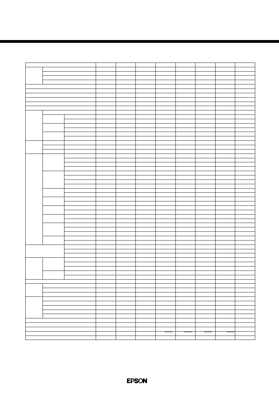
8
E0C88F360
q List of Different Specifications between E0C88F360 and E0C88xxx
E0C88348
×
q
×
–
48KB
2KB
10
9
8
q
×
q
2.4 ~ 5.5V
3.5 ~ 5.5V
1.8 ~ 3.5V
30k ~ 50kHz
30k ~ 4.1MHz
30k ~ 8.2MHz
-40 ~ 85
°C
18
A
1.0mA
1
A
VD1
VDD
VD1
×
16 levels
2 ch.
×
R26/FR
R51/BACK
Package
QFP18-176pin
QFP8-160pin
QFP8-128pin
QFP15-128pin
Number of additional pin for Flash
ROM size
RAM size
Input port
Output port
I/O port
Chip mode
Single chip
Extended 64K
MCU
MPU
Extended
MCU
512K min.
MPU
Extended
MCU
512K max.
MPU
Operating
Normal
(VD1 = 2.2V)
mode
High-speed
(VD1 = 3.3V)
Low-power
(VD1 = 1.3V)
Mask ROM
OSC1
Crystal
option select
External
CR
Crystal (with CG)
OSC3
Crystal
Ceramic
CR
External
I/O (P) port
With resistor
pull-up
Gate direct
Input (K) port
With resistor
pull-up
Gate direct
Output (R) port
Complementary
output spec.
Nch open drain
LCD duty
1/32 & 1/16
1/8
LCD power
TYPE A (4.5V)
TYPE B (5.5V)
External power source
Reset
K0 port combination
SVD reset
Operating voltage
Normal
High-speed
Low-power
Operating
OSC1
Normal
frequency
High-speed
Low-power
OSC3
Normal
High-speed
Operating temperature
Power
Normal (5.5V, 32kHz)
current
High-speed (5.5V, 1MHz)
(max.)
Sleep mode (5.5V, normal mode)
Power
CPU
supply
Peripheral
Port
OSC
PROM
SVD
Analog comparator
A/D converter
R26 output port specification
R51 output port specification
E0C88316/317
×
q
×
–
16KB
2KB
←
q
←
×
←
×
R26/FR
R51/BACK
E0C88308
×
q
×
–
8KB
256B
9
5
←
q
←
×
←
×
R26/FR
R51/BACK
E0C88862
×
q
–
60KB
1.5KB
←
2
←
q
←
TBD
←
VOSC
×
←
×
R26/TOUT
R51/BZ
E0C88861
×
q
–
60KB
1.5KB
←
2
←
q
←
TBD
←
VD1
×
←
×
R26/TOUT
R51/BZ
E0C88832
×
q
–
32KB
1.5KB
←
2
←
q
←
TBD
←
×
←
×
R26/TOUT
R51/BZ
E0C88F360
q
×
5 pins
60KB
2KB
10
9
8
q
×
q
×
q
×
q
×
q
×
q
×
q
×
q
×
←
← 1
←
-20 ~ 70
°C
25
A
2.0mA
1
A
←
VD1
←
2 ch.
4 ch., 10 bits
R26/FR/TOUT
R51/BACK/BZ
E0C88P348
q
×
5 pins
48KB
2KB
10
9
8
q
×
q
×
q
×
q
×
q
×
q
×
q
×
q
×
q
×
q
×
q
×
3.3 ~ 5.5V
4.5 ~ 5.5V
×
←
×
←
30k ~ 6MHz
0 ~ 70
°C
12mA
15mA
1
A
VDD
←
VDD
8 levels
×
R26/FR
R51/BACK
q = Available,
× = Not available
1: The E0C88F360 operating voltage range (1.8V to 3.5V) in Low-power mode may be modified.
Notes: The pin assignment of the E0C88F360 is incompatible with the E0C883xx and E0C888xx.
The table does not contain some different items. Refer to the manuals of the E0C88F360 and the E0C88xxx.
相關(guān)PDF資料 |
PDF描述 |
|---|---|
| E112PD040D040SG | INTERCONNECTION DEVICE |
| E1SAA18-16.670MTR | QUARTZ CRYSTAL RESONATOR, 16.67 MHz |
| E1SAA18-3.686M | QUARTZ CRYSTAL RESONATOR, 3.686 MHz |
| E1SAD12-24.000MTR | QUARTZ CRYSTAL RESONATOR, 24 MHz |
| E1SAD18-33.3333MTR | QUARTZ CRYSTAL RESONATOR, 33.3333 MHz |
相關(guān)代理商/技術(shù)參數(shù) |
參數(shù)描述 |
|---|---|
| E0D2P7BP05T WAF | 制造商:ON Semiconductor 功能描述: |
| E0D3P9BP05T WAF | 制造商:ON Semiconductor 功能描述: |
| E0D4P3BP05T WAF | 制造商:ON Semiconductor 功能描述: |
| E0D4P7BP05T WAF | 制造商:ON Semiconductor 功能描述: |
| E0D5P6BP05TZ WAF | 制造商:ON Semiconductor 功能描述: |
發(fā)布緊急采購,3分鐘左右您將得到回復(fù)。