- 您現(xiàn)在的位置:買賣IC網(wǎng) > PDF目錄384279 > EDD51321CBH-7ETT-E (ELPIDA MEMORY INC) 512M bits DDR SDRAM PDF資料下載
參數(shù)資料
| 型號: | EDD51321CBH-7ETT-E |
| 廠商: | ELPIDA MEMORY INC |
| 元件分類: | DRAM |
| 英文描述: | 512M bits DDR SDRAM |
| 中文描述: | 16M X 32 SYNCHRONOUS DRAM, 6 ns, PBGA90 |
| 封裝: | ROHS COMPLIANT, FBGA-90 |
| 文件頁數(shù): | 7/55頁 |
| 文件大?。?/td> | 589K |
| 代理商: | EDD51321CBH-7ETT-E |
第1頁第2頁第3頁第4頁第5頁第6頁當前第7頁第8頁第9頁第10頁第11頁第12頁第13頁第14頁第15頁第16頁第17頁第18頁第19頁第20頁第21頁第22頁第23頁第24頁第25頁第26頁第27頁第28頁第29頁第30頁第31頁第32頁第33頁第34頁第35頁第36頁第37頁第38頁第39頁第40頁第41頁第42頁第43頁第44頁第45頁第46頁第47頁第48頁第49頁第50頁第51頁第52頁第53頁第54頁第55頁
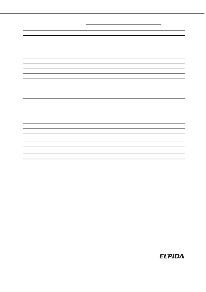
EDD51321CBH
Preliminary Data Sheet E1094E30 (Ver. 3.0)
7
-6C
-7E
Parameter
Symbol
min.
max.
min.
max.
Unit
Notes
Write postamble
tWPST
0.4
0.6
0.4
0.6
tCK
7
Write command to first DQS latching
transition
tDQSS
0.75
1.25
0.75
1.25
tCK
DQS falling edge to CK setup time
tDSS
0.2
—
0.2
—
tCK
DQS falling edge hold time from CK
tDSH
0.2
—
0.2
—
tCK
DQS input high pulse width
tDQSH
0.35
—
0.35
—
tCK
DQS input low pulse width
tDQSL
0.35
—
0.35
—
tCK
Address and control input setup time tIS
1.1
—
1.3
—
ns
3
Address and control input hold time
tIH
1.1
—
1.3
—
ns
3
Address and control input pulse width tIPW
2.7
—
3.0
—
ns
3
Mode register set command cycle
time
tMRD
2
—
2
—
tCK
Active to Precharge command period tRAS
42
120000
45
120000
ns
Active to Active/Auto-refresh
command period
Auto-refresh to Active/Auto-refresh
command period
tRC
66
—
75
—
ns
tRFC
108
—
108
—
ns
Active to Read/Write delay
tRCD
24
—
30
—
ns
Precharge to active command period tRP
24
—
22.5
—
ns
Column address to column address
delay
tCCD
1
—
1
—
tCK
Active to active command period
tRRD
12
—
15
—
ns
Write recovery time
tWR
15
—
15
—
ns
Autoprecharge write recovery and
precharge time
tDAL
tWR + tRP
—
tWR + tRP
—
ns
Self-Refresh Exit Period
tSREX
120
—
120
—
ns
Internal Write to Read command
delay
tWTR
2
—
1
—
tCK
Average periodic refresh interval
tREF
—
7.8
—
7.8
μs
Notes: 1. On all AC measurements, we assume the test conditions shown in “Test conditions” and full driver
strength is assumed for the output load, that is both A6 and A5 of EMRS is set to be “L”.
2. This parameter defines the signal transition delay from the cross point of CK and /CK. The signal
transition is defined to occur when the signal level crossing VDDQ/2.
3. The timing reference level is VDDQ/2.
4. Output valid window is defined to be the period between two successive transition of data out signals.
The signal transition is defined to occur when the signal level crossing VDDQ/2.
5. tHZ is defined as DOUT transition delay from low-Z to high-Z at the end of read burst operation. The
timing reference is cross point of CK and /CK. This parameter is not referred to a specific DOUT voltage
level, but specify when the device output stops driving.
6. tLZ is defined as DOUT transition delay from high-Z to low-Z at the beginning of read operation. This
parameter is not referred to a specific DOUT voltage level, but specify when the device output begins
driving.
7. The transition from low-Z to high-Z is defined to occur when the device output stops driving. A specific
reference voltage to judge this transition is not given.
8. tAC, tDQSCK, tHZ and tLZ are specified with 15pF bus loading conditio
n.
相關PDF資料 |
PDF描述 |
|---|---|
| EDE1116ABSE-6E-E | 1G bits DDR2 SDRAM |
| EDE1104ABSE | 1G bits DDR2 SDRAM |
| EDE1104ABSE-4A-E | 1G bits DDR2 SDRAM |
| EDE1104ABSE-5C-E | 1G bits DDR2 SDRAM |
| EDE1104ABSE-6C-E | 1G bits DDR2 SDRAM |
相關代理商/技術參數(shù) |
參數(shù)描述 |
|---|---|
| EDD51321DBH-5BTS-F | 制造商:ELPIDA 制造商全稱:Elpida Memory 功能描述:512M bits DDR Mobile RAM? WTR (Wide Temperature Range) |
| EDD51321DBH-6ETS-F | 制造商:ELPIDA 制造商全稱:Elpida Memory 功能描述:512M bits DDR Mobile RAM? WTR (Wide Temperature Range) |
| EDD51321DBH-TS | 制造商:ELPIDA 制造商全稱:Elpida Memory 功能描述:512M bits DDR Mobile RAM? WTR (Wide Temperature Range) |
| EDD51323DBH-5BLS-F | 制造商:ELPIDA 制造商全稱:Elpida Memory 功能描述:512M bits DDR Mobile RAM? WTR (Wide Temperature Range), Low Power Function |
| EDD51323DBH-6ELS-F | 制造商:ELPIDA 制造商全稱:Elpida Memory 功能描述:512M bits DDR Mobile RAM? WTR (Wide Temperature Range), Low Power Function |
發(fā)布緊急采購,3分鐘左右您將得到回復。