- 您現(xiàn)在的位置:買賣IC網(wǎng) > PDF目錄371904 > HUF75309T3ST (INTERSIL CORP) 3A, 55V, 0.070 Ohm, N-Channel UltraFET Power MOSFET PDF資料下載
參數(shù)資料
| 型號: | HUF75309T3ST |
| 廠商: | INTERSIL CORP |
| 元件分類: | JFETs |
| 英文描述: | 3A, 55V, 0.070 Ohm, N-Channel UltraFET Power MOSFET |
| 中文描述: | 3 A, 55 V, 0.07 ohm, N-CHANNEL, Si, POWER, MOSFET |
| 文件頁數(shù): | 2/8頁 |
| 文件大?。?/td> | 88K |
| 代理商: | HUF75309T3ST |
24
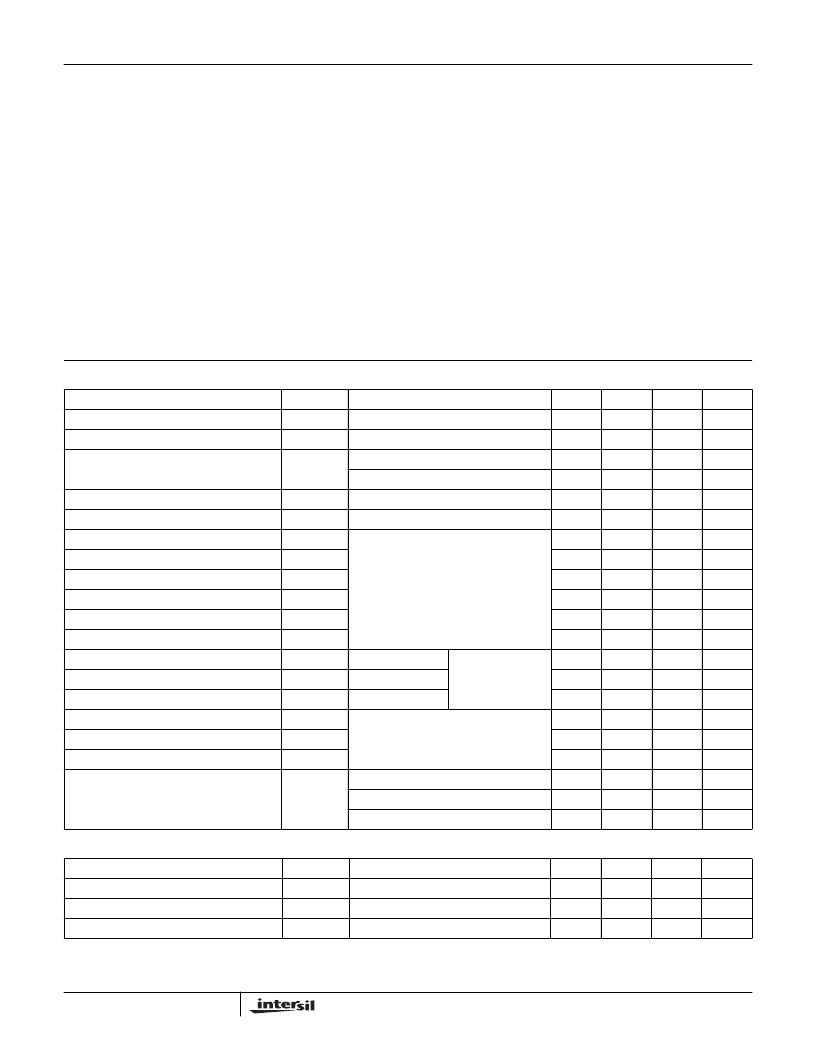
Absolute Maximum Ratings
T
A
= 25
o
C, Unless Otherwise Specified
HUF75309T3ST
55
55
±
20V
UNITS
V
V
V
Drain to Source Voltage (Note 1). . . . . . . . . . . . . . . . . . . . . . . . . . . . . . . . . . . . . . . . . . V
DSS
Drain to Gate Voltage (R
GS
= 20k
) (Note 1) . . . . . . . . . . . . . . . . . . . . . . . . . . . . . . . .V
DGR
Gate to Source Voltage . . . . . . . . . . . . . . . . . . . . . . . . . . . . . . . . . . . . . . . . . . . . . . . . . . V
GS
Drain Current
Continuous (Note 2) (Figure 2). . . . . . . . . . . . . . . . . . . . . . . . . . . . . . . . . . . . . . . . . . . . . I
D
Pulsed Drain Current . . . . . . . . . . . . . . . . . . . . . . . . . . . . . . . . . . . . . . . . . . . . . . . . . . .I
DM
Pulsed Avalanche Rating. . . . . . . . . . . . . . . . . . . . . . . . . . . . . . . . . . . . . . . . . . . . . . . . . E
AS
Power Dissipation (Note 2) . . . . . . . . . . . . . . . . . . . . . . . . . . . . . . . . . . . . . . . . . . . . . . . . P
D
Derate Above 25
o
C . . . . . . . . . . . . . . . . . . . . . . . . . . . . . . . . . . . . . . . . . . . . . . . . . . . . . . .
Operating and Storage Temperature . . . . . . . . . . . . . . . . . . . . . . . . . . . . . . . . . . . . T
J
, T
STG
Maximum Temperature for Soldering
Leads at 0.063in (1.6mm) from Case for 10s. . . . . . . . . . . . . . . . . . . . . . . . . . . . . . . . . .T
L
Package Body for 10s, See Techbrief 334 . . . . . . . . . . . . . . . . . . . . . . . . . . . . . . . . . . T
pkg
CAUTION: Stresses above those listed in “Absolute Maximum Ratings” may cause permanent damage to the device. This is a stress only rating and operation of the
device at these or any other conditions above those indicated in the operational sections of this specification is not implied.
3
Figure 5
A
Figures 6, 14, 15
1.1
9.09
-55 to 150
W
mW/
o
C
o
C
300
260
o
C
o
C
NOTE:
1. T
J
= 25
o
C to 125
o
C.
Electrical Specifications
T
A
= 25
o
C, Unless Otherwise Specified
PARAMETER
SYMBOL
TEST CONDITIONS
MIN
TYP
MAX
UNITS
Drain to Source Breakdown Voltage
BV
DSS
V
GS(TH)
I
DSS
I
D
= 250
μ
A, V
GS
= 0V (Figure 11)
V
GS
= V
DS
, I
D
= 250
μ
A (Figure 10)
V
DS
= 50V, V
GS
= 0V
V
DS
= 45V, V
GS
= 0V, T
A
= 150
o
C
V
GS
=
±
20V
I
D
= 3A, V
GS
= 10V (Figure 9)
V
DD
= 30V, I
D
3A, R
L
= 10
,
V
GS
=
10V, R
GS
= 28
55
-
-
V
Gate to Source Threshold Voltage
2
-
4
V
Zero Gate Voltage Drain Current
-
-
1
μ
A
-
-
250
μ
A
Gate to Source Leakage Current
I
GSS
r
DS(ON)
t
ON
t
d(ON)
t
r
t
d(OFF)
t
f
t
OFF
Q
g(TOT)
Q
g(10)
Q
g(TH)
C
ISS
C
OSS
C
RSS
R
θ
JA
-
-
100
nA
Drain to Source On Resistance
-
0.057
0.070
Turn-On Time
-
-
45
ns
Turn-On Delay Time
-
8
-
ns
Rise Time
-
20
-
ns
Turn-Off Delay Time
-
12
-
ns
Fall Time
-
28
-
ns
Turn-Off Time
-
-
65
ns
Total Gate Charge
V
GS
= 0V to 20V
V
GS
= 0V to 10V
V
GS
= 0V to 2V
V
DS
= 25V, V
GS
= 0V, f = 1MHz
(Figure 12)
V
DD
= 30V, I
D
3A,
R
L
= 10
I
g(REF)
= 1.0mA
(Figure 13)
-
19
23
nC
Gate Charge at 10V
-
10.7
13
nC
Threshold Gate Charge
-
0.71
0.85
nC
Input Capacitance
-
352
-
pF
Output Capacitance
-
146
-
pF
Reverse Transfer Capacitance
-
30
-
pF
Thermal Resistance Junction to Ambient
Pad Area = 0.164 in
2
(See note 2)
Pad Area = 0.068 in
2
(See TB337)
Pad Area = 0.026 in
2
(See TB337)
-
-
110
o
C/W
o
C/W
o
C/W
-
-
126
-
-
143
Source to Drain Diode Specifications
PARAMETER
SYMBOL
TEST CONDITIONS
MIN
TYP
MAX
UNITS
Source to Drain Diode Voltage
V
SD
t
rr
Q
RR
I
SD
= 3A
I
SD
= 3A, dI
SD
/dt = 100A/
μ
s
I
SD
= 3A, dI
SD
/dt = 100A/
μ
s
-
-
1.25
V
Reverse Recovery Time
-
-
41
ns
Reverse Recovered Charge
-
-
59
nC
NOTE:
2. 110
o
C/W measured using FR-4 board with 0.164 in
2
footprint for 1000 seconds.
HUF75309T3ST
相關(guān)PDF資料 |
PDF描述 |
|---|---|
| HUF75309T3ST | 3A, 55V, 0.070 Ohm, N-Channel UltraFET Power MOSFET |
| HUF75329S3S | 49A, 55V, 0.024 Ohm, N-Channel UltraFET Power MOSFETs |
| HUF75329P3 | 49A, 55V, 0.024 Ohm, N-Channel UltraFET Power MOSFETs |
| HUF75329G3 | 49A, 55V, 0.024 Ohm, N-Channel UltraFET Power MOSFETs(49A, 55V, 0.024Ω, N溝道UltraFET功率MOS場效應(yīng)管) |
| HUF75329D3S | 20A, 55V, 0.026 Ohm, N-Channel UltraFET Power MOSFETs |
相關(guān)代理商/技術(shù)參數(shù) |
參數(shù)描述 |
|---|---|
| HUF75321D3 | 功能描述:MOSFET 20a 55V N-Channel UltraFET RoHS:否 制造商:STMicroelectronics 晶體管極性:N-Channel 汲極/源極擊穿電壓:650 V 閘/源擊穿電壓:25 V 漏極連續(xù)電流:130 A 電阻汲極/源極 RDS(導(dǎo)通):0.014 Ohms 配置:Single 最大工作溫度: 安裝風(fēng)格:Through Hole 封裝 / 箱體:Max247 封裝:Tube |
| HUF75321D3 | 制造商:Fairchild Semiconductor Corporation 功能描述:MOSFET N I-PAK |
| HUF75321D3S | 功能描述:MOSFET 20a 55V N-Channel UltraFET RoHS:否 制造商:STMicroelectronics 晶體管極性:N-Channel 汲極/源極擊穿電壓:650 V 閘/源擊穿電壓:25 V 漏極連續(xù)電流:130 A 電阻汲極/源極 RDS(導(dǎo)通):0.014 Ohms 配置:Single 最大工作溫度: 安裝風(fēng)格:Through Hole 封裝 / 箱體:Max247 封裝:Tube |
| HUF75321D3ST | 功能描述:MOSFET 20a 55V N-Channel UltraFET RoHS:否 制造商:STMicroelectronics 晶體管極性:N-Channel 汲極/源極擊穿電壓:650 V 閘/源擊穿電壓:25 V 漏極連續(xù)電流:130 A 電阻汲極/源極 RDS(導(dǎo)通):0.014 Ohms 配置:Single 最大工作溫度: 安裝風(fēng)格:Through Hole 封裝 / 箱體:Max247 封裝:Tube |
| HUF75321D3ST_S2457 | 制造商:Rochester Electronics LLC 功能描述:- Bulk |
發(fā)布緊急采購,3分鐘左右您將得到回復(fù)。