- 您現(xiàn)在的位置:買賣IC網(wǎng) > PDF目錄370781 > HYB18T256160AL-3S (INFINEON TECHNOLOGIES AG) 256 Mbi t DDR2 SDRAM PDF資料下載
參數(shù)資料
| 型號(hào): | HYB18T256160AL-3S |
| 廠商: | INFINEON TECHNOLOGIES AG |
| 英文描述: | 256 Mbi t DDR2 SDRAM |
| 中文描述: | 256姆噸DDR2內(nèi)存 |
| 文件頁(yè)數(shù): | 29/90頁(yè) |
| 文件大小: | 1246K |
| 代理商: | HYB18T256160AL-3S |
第1頁(yè)第2頁(yè)第3頁(yè)第4頁(yè)第5頁(yè)第6頁(yè)第7頁(yè)第8頁(yè)第9頁(yè)第10頁(yè)第11頁(yè)第12頁(yè)第13頁(yè)第14頁(yè)第15頁(yè)第16頁(yè)第17頁(yè)第18頁(yè)第19頁(yè)第20頁(yè)第21頁(yè)第22頁(yè)第23頁(yè)第24頁(yè)第25頁(yè)第26頁(yè)第27頁(yè)第28頁(yè)當(dāng)前第29頁(yè)第30頁(yè)第31頁(yè)第32頁(yè)第33頁(yè)第34頁(yè)第35頁(yè)第36頁(yè)第37頁(yè)第38頁(yè)第39頁(yè)第40頁(yè)第41頁(yè)第42頁(yè)第43頁(yè)第44頁(yè)第45頁(yè)第46頁(yè)第47頁(yè)第48頁(yè)第49頁(yè)第50頁(yè)第51頁(yè)第52頁(yè)第53頁(yè)第54頁(yè)第55頁(yè)第56頁(yè)第57頁(yè)第58頁(yè)第59頁(yè)第60頁(yè)第61頁(yè)第62頁(yè)第63頁(yè)第64頁(yè)第65頁(yè)第66頁(yè)第67頁(yè)第68頁(yè)第69頁(yè)第70頁(yè)第71頁(yè)第72頁(yè)第73頁(yè)第74頁(yè)第75頁(yè)第76頁(yè)第77頁(yè)第78頁(yè)第79頁(yè)第80頁(yè)第81頁(yè)第82頁(yè)第83頁(yè)第84頁(yè)第85頁(yè)第86頁(yè)第87頁(yè)第88頁(yè)第89頁(yè)第90頁(yè)

HYB18T256400/800/160AF
256Mb DDR2 SDRAM
INFINEON Technologies
Page 29 Rev. 1.02 May 2004
2.6 Read and Write Commands and Access Modes
After a bank has been activated, a read or write cycle can be executed. This is accomplished by setting RAS high,
CS and CAS low at the clock’s rising edge. WE must also be defined at this time to determine whether the access
cycle is a read operation (WE high) or a write operation (WE low). The DDR2 SDRAM provides a wide variety of
fast access modes. A single Read or Write Command will initiate a serial read or write operation on successive
clock cycles at data rates of up to 667Mb/sec/pin for main memory. The boundary of the burst cycle is restricted to
specific segments of the page length.
For example, the 16Mbit x 4 I/O x 4 Bank chip has a page length of 2048 bits (defined by CA0-CA9 & CA11).
In case of a 4-bit burst operation (burst length = 4) the page length of 2048 is divided into 512 uniquely address-
able segments (4-bits x 4 I/O each). The 4-bit burst operation will occur entirely within one of the 512 segments
(defined by CA0-CA8) beginning with the column address supplied to the device during the Read or Write Com-
mand (CA0-CA9 & A11). The second, third and fourth access will also occur within this segment, however, the
burst order is a function of the starting address, and the burst sequence.
In case of a 8-bit burst operation (burst length = 8) the page length of 2048 is divided into 256 uniquely address-
able double segments (8-bits x 4 I/O each). The 8-bit burst operation will occur entirely within one of the 256 dou-
ble segments (defined by CA0-CA7) beginning with the column address supplied to the device during the Read or
Write Command (CA0-CA9 & CA11).
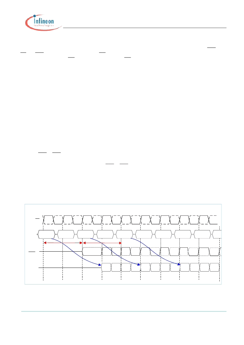
A new burst access must not interrupt the previous 4 bit burst operation in case of BL = 4 setting. Therefore the
minimum CAS to CAS delay (tCCD) is a minimum of 2 clocks for read or write cycles
.
For 8 bit burst operation (BL = 8) the minimum CAS to CAS delay (tCCD) is 4 clocks for read or write cycles.
Burst interruption is allowed with 8 bit burst operation. For details see the “Burst Interrupt” - Section of this
datasheet.
Example:
Read Burst Timing Example: (CL = 3, AL = 0, RL = 3, BL = 4)
NOP
NOP
NOP
NOP
NOP
READ A
T0
T2
T1
T3
T4
T5
T6
T7
T12
CMD
DQ
RB
DQS,
DQS
READ B
NOP
Dout A0
Dout A1
Dout A2
Dout A3 Dout B0
Dout B1
Dout B2
Dout B3
Dout C0
Dout C1
Dout C2
Dout C3
NOP
READ C
tCCD
tCCD
CK, CK
相關(guān)PDF資料 |
PDF描述 |
|---|---|
| HYB18T256400AF | 256 Mbi t DDR2 SDRAM |
| HYB18T256400AF-3 | 256 Mbi t DDR2 SDRAM |
| HYB18T256400AF-37 | 256 Mbi t DDR2 SDRAM |
| HYB18T256400AF-3S | 256 Mbi t DDR2 SDRAM |
| HYB18T256400AF-5 | 256 Mbi t DDR2 SDRAM |
相關(guān)代理商/技術(shù)參數(shù) |
參數(shù)描述 |
|---|---|
| HYB18T256400AF-3.7 | 制造商:Infineon Technologies AG 功能描述:64M X 4 DDR DRAM, 0.5 ns, PBGA60 |
| HYB18T256400AF-5 | 制造商:Infineon Technologies AG 功能描述:SDRAM, DDR, 64M x 4, 60 Pin, Plastic, BGA |
| HYB18T256800AF-5 | 制造商:Infineon Technologies AG 功能描述: |
| HYB18T512161BF-25 | 制造商:Qimonda 功能描述:SDRAM, DDR, 32M x 16, 84 Pin, Plastic, BGA |
| HYB18T512400AF-5 | 制造商:Intersil Corporation 功能描述:SDRAM, DDR, 128M x 4, 60 Pin, Plastic, BGA |
發(fā)布緊急采購(gòu),3分鐘左右您將得到回復(fù)。