- 您現(xiàn)在的位置:買(mǎi)賣(mài)IC網(wǎng) > PDF目錄360744 > ICS1889 100Base-FX Integrated PHYceiverTM PDF資料下載
參數(shù)資料
| 型號(hào): | ICS1889 |
| 英文描述: | 100Base-FX Integrated PHYceiverTM |
| 中文描述: | 100Base - FX光纖綜合PHYceiverTM |
| 文件頁(yè)數(shù): | 6/35頁(yè) |
| 文件大小: | 1096K |
| 代理商: | ICS1889 |
第1頁(yè)第2頁(yè)第3頁(yè)第4頁(yè)第5頁(yè)當(dāng)前第6頁(yè)第7頁(yè)第8頁(yè)第9頁(yè)第10頁(yè)第11頁(yè)第12頁(yè)第13頁(yè)第14頁(yè)第15頁(yè)第16頁(yè)第17頁(yè)第18頁(yè)第19頁(yè)第20頁(yè)第21頁(yè)第22頁(yè)第23頁(yè)第24頁(yè)第25頁(yè)第26頁(yè)第27頁(yè)第28頁(yè)第29頁(yè)第30頁(yè)第31頁(yè)第32頁(yè)第33頁(yè)第34頁(yè)第35頁(yè)
6
ICS1889
Line Transmitter
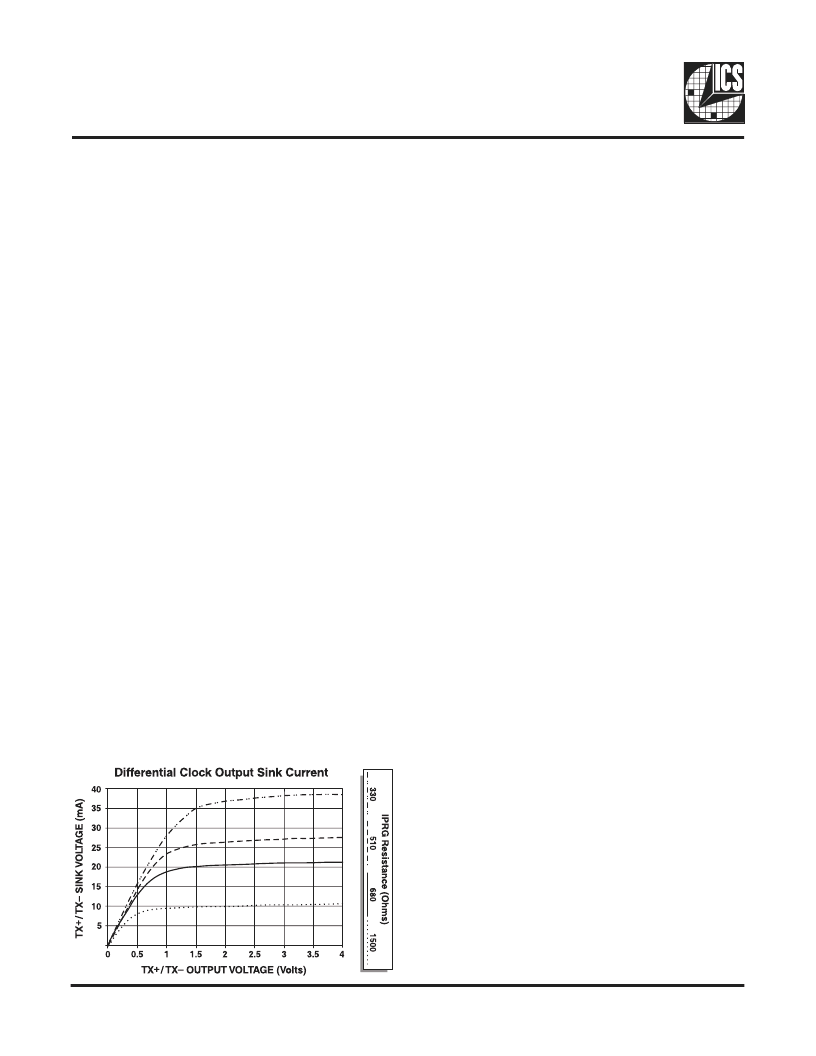
The Line Transmitter output pair is a differential positive ECL
(PECL) interface designed to connect directly to a standard
fiber optic transceiver. The differential driver for the transmit
signal is a programmable current source designed for resistive
termination. Using an external resistor connected to the IPRG
pin, the output current may be preset.
The differential driver for the TX
±
is current mode and is
designed to drive resistive terminations in a complementary
fashion. The output is current-sinking only, with the amount
of sink current programmable via the
IPRG1
pin. The sink
current is equal to four times the IPRG1 current. For most
applications, an 910
resistor from VDD to IPRG1 will set
the current to the necessary precision.
The TX
±
pins are incapable for sourcing current, so V
OH
must
be set by the ratios of the Thevenin termination resistors for
each of the lines. R1 is a pull-up resistor connected from the
PECL output to VDD. R2 is a pull-down resistor connected
from the PECL output to VSS. R1 and R2 are electrically in
parallel from an AC standpoint. If we pick a target impedance
of 50
for our transmission line impedance, a value of 62
for R1 and a value of 300
for R2 would yield a Thevenin
equivalent characteristic impedance of 49.7
and a V
OH
value of V
DD
-.88 volts, compatible with PECL circuits.
To set a value for V
OL
, we must determine a value for I
prg
that will cause the output FETs to sink an appropriate current.
We desire V
OL
to be V
DD
-1.81 or greater. Setting up a sink
current of 19 milliamperes would guarantee this through our
output termination resistors. As this is controlled by
4/1 current mirror, 4.75mA into I
prg
should set this current
properly. A 910
resistor from V
DD
to I
prg
should work fine.
Line Receiver
The Line Receiver is a differential input pair designed to
interface directly to a standard fiber optic transceiver. It is a
differential PECL input buffer.
Signal Error Detector
The
ICS1889
Signal Error Detector is part of the clock
recovery PLL. It detects a Receive Signal Error if no receive
signal is received and detects a PLL Lock Error if the PLL is
unable to lock on to the receive channel signal. A receive
channel error is defined as the loss of receive signal or the loss
of PLL lock.
Remote Fault Signaling
Remote fault signaling allows a node to indicate receive
channel errors to its Link Partner using its transmit channel.
When used by both nodes on a link segment, the integrity of
both the transmit and receive channels can be verified.
Since 100Base-FX systems do not use auto-negotiation, an
alternative, in-band signaling scheme is used to signal remote
fault conditions. This scheme, Far End Fault Indication, relies
on the characteristics of the quiescent state, (a continuous
IDLE stream). The IDLE stream is a continuous stream of
logic ones and a carrier is defined as the receipt of two
noncontiguous logic zeroes. A Far End Fault is signaled with
84 logic ones followed by one logic zero, with the pattern
repeated at least three times.
A Far End Fault will be signaled under three conditions; the
first is when no activity is received from the Link Partner,
since this can indicate a broken receive wire. The second is
when the clock recovery circuit detects a Receive Signal Error
or PLL Lock Error. The third is when a management entity
sets the Transmit Far End Fault bit (16:3).
Far End Fault signaling continues until the condition causing
the fault ceases.
Far End Fault Detection
The Far End Fault detector monitors the receive data serial bit
stream looking for a repetitive pattern of 84 logic ones
followed by a logic zero. Non-ICS1889 PHYs may have
different definitions of what constitutes a remote fault.
However, an
ICS1889
will always respond to the in-band
error signaling scheme. If the
ICS1889
detects three
consecutive patterns described above, it will signal a far end
fault to the Link Monitor.
Link Monitor
If the Link Monitor receives a far end fault indication or a
local receive channel error, it causes the
ICS1889
to enter the
IDLE mode, isolate the MII and assert the Link Status bit in
the Status Register. Once the far end fault condition is de-
asserted, the Link Monitor will return to the Link OK
condition if the local receive channel is clear of errors. Once
detected, a receive channel error signal will be indicated from
330 to 1000 microseconds.
相關(guān)PDF資料 |
PDF描述 |
|---|---|
| ICS1892 | 10Base-T/100Base-TX Integrated PHYceiver |
| ICS1892Y | 10Base-T/100Base-TX Integrated PHYceiver |
| ICS1892Y-10 | 10Base-T/100Base-TX Integrated PHYceiver |
| ICS1892Y-14 | 10Base-T/100Base-TX Integrated PHYceiver |
| ICS1893AF | 3.3V 10Base-T/100Base-TX Integrated PHYceiverTM |
相關(guān)代理商/技術(shù)參數(shù) |
參數(shù)描述 |
|---|---|
| ICS1890 | 制造商:ICS 制造商全稱:ICS 功能描述:Auto-Negotiation Advertisement Register (register 4 [0x04]) |
| ICS1890Y | 制造商:ICS 功能描述: 制造商:ICS 功能描述:LAN Transceiver, Single, 64 Pin, Plastic, QFP 制造商:ICS 功能描述:1890Y-4 制造商:Integrated Device Technology Inc 功能描述:LAN Transceiver, Single, 64 Pin, Plastic, QFP |
| ICS1890Y-14 | 制造商:ICS 制造商全稱:ICS 功能描述:Auto-Negotiation Advertisement Register (register 4 [0x04]) |
| ICS1890Y-4 | 制造商:ICS 功能描述:1890Y-4 |
| ICS1891 | 制造商:未知廠家 制造商全稱:未知廠家 功能描述:LAN Transceiver |
發(fā)布緊急采購(gòu),3分鐘左右您將得到回復(fù)。