- 您現(xiàn)在的位置:買賣IC網(wǎng) > PDF目錄377484 > IDT77V1254L25L25PG (Integrated Device Technology, Inc.) Quad Port PHY (Physical Layer) for 25.6 and 51.2 ATM Networks PDF資料下載
參數(shù)資料
| 型號: | IDT77V1254L25L25PG |
| 廠商: | Integrated Device Technology, Inc. |
| 英文描述: | Quad Port PHY (Physical Layer) for 25.6 and 51.2 ATM Networks |
| 中文描述: | 四端口PHY(實體層)為25.6和51.2 ATM網(wǎng)絡(luò) |
| 文件頁數(shù): | 5/47頁 |
| 文件大小: | 840K |
| 代理商: | IDT77V1254L25L25PG |
第1頁第2頁第3頁第4頁當(dāng)前第5頁第6頁第7頁第8頁第9頁第10頁第11頁第12頁第13頁第14頁第15頁第16頁第17頁第18頁第19頁第20頁第21頁第22頁第23頁第24頁第25頁第26頁第27頁第28頁第29頁第30頁第31頁第32頁第33頁第34頁第35頁第36頁第37頁第38頁第39頁第40頁第41頁第42頁第43頁第44頁第45頁第46頁第47頁
5 of 47
September 21, 2001
IDT77V1254L25
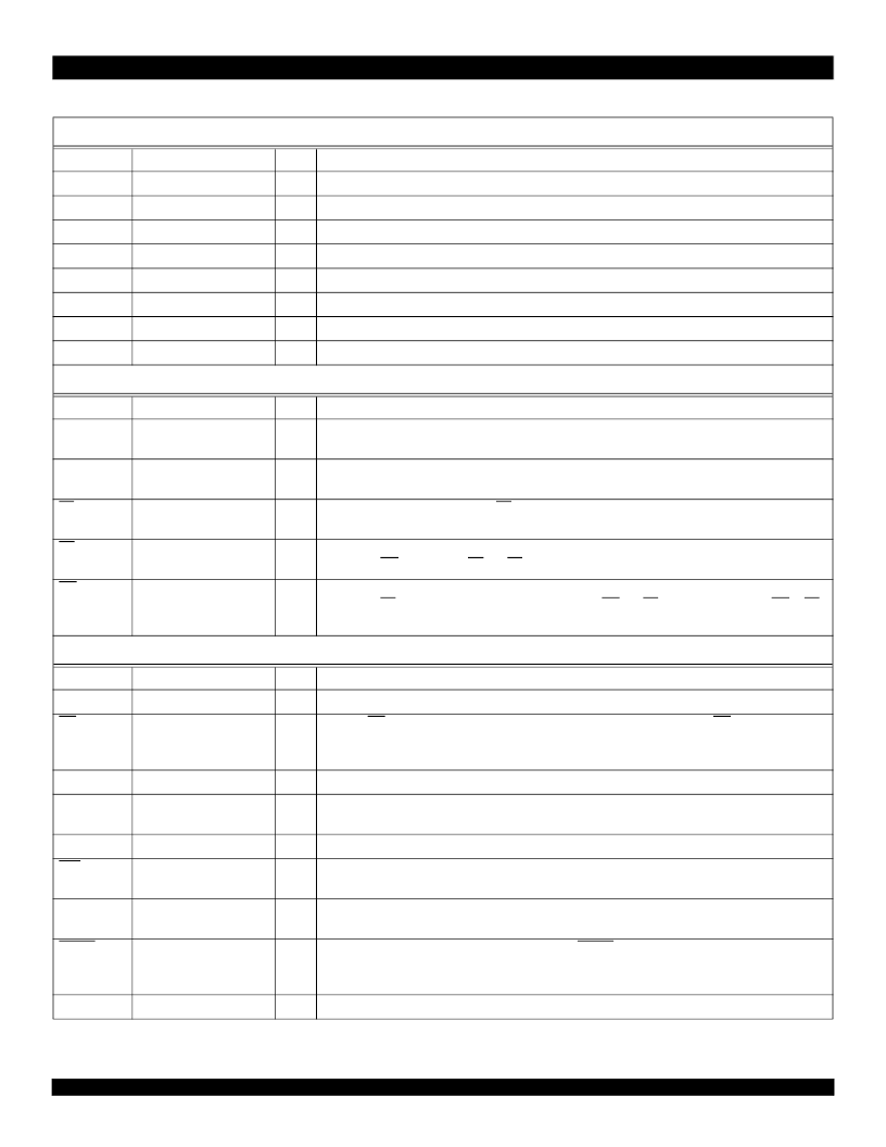
Signal Descriptions
Line Side Signals
Signal Name
Pin Number
I/O
Signal Description
RX0+,-
139, 138
In
Port 0 positive and negative receive differential input pair.
RX1+,-
133, 132
In
Port 1 positive and negative receive differential input pair.
RX2+,-
121, 120
In
Port 2 positive and negative receive differential input pair.
RX3+,-
115, 114
In
Port 3 positive and negative receive differential input pair.
TX0+,-
4, 3
Out
Port 0 positive and negative transmit differential output pair.
TX1+,-
144, 143
Out
Port 1 positive and negative transmit differential output pair.
TX2+,-
110, 109
Out
Port 2 positive and negative transmit differential output pair.
TX3+,-
106, 105
Out
Port 3 positive and negative transmit differential output pair.
Utility Bus Signals
Signal Name
Pin Number
I/O
Signal Description
AD[7:0]
101, 100, 99, 98, 96, 95, 94,
93
In/Out
Utility bus address/data bus. The address input is sampled on the falling edge of ALE. Data is output on this
bus when a read is performed. Input data is sampled at the completion of a write operation.
ALE
91
In
Utility bus address latch enable. Asynchronous input. An address on the AD bus is sampled on the falling
edge of ALE. ALE must be low when the AD bus is being used for data.
CS
90
Utility bus asynchronous chip select. CS must be asserted to read or write an internal register. It may remain
asserted at all times if desired
RD
89
In
Utility bus read enable. Active low asynchronous input. After latching an address, a read is performed by
deasserting WR and asserting RD and CS.
WR
88
In
Utility bus write enable. Active low asynchronous input. After latching an address, a write is performed by
deasserting RD, placing data on the AD bus, and asserting WR and CS. Data is sampled when WR or CS is
deasserted.
Miscellaneous Signals
Signal Name
Pin Number
I/O
Signal Description
DA
103
In
Reserved signal. This input must be connected to logic low.
INT
85
Out
Interrupt. INT is an open-drain output, driven low to indicate an interrupt. Once low, INT remains low until the
interrupt status in the appropriate interrupt Status Register is read. Interrupt sources are programmable via
the interrupt Mask Registers.
MM
6
In
Reserved signal. This input must be connected to logic low.
MODE[1:0]
7, 8
In
Mode Selects. They determine the configuration of the PHY/ATM interface. 00 = UTOPIA Level 2. 01 = UTO-
PIA Level 1. 10 = DPI. 11 is reserved.
OSC
126
In
TTL line rate clock source, driven by a 100 ppm oscillator. 32 MHz for 25.6 Mbps; 64 MHz for 51.2 Mbps.
RST
87
In
Reset. Active low asynchronous input resets all control logic, counters and FIFOs. A reset must be per-
formed after power up prior to normal operation of the part.
RXLED[3:0]
82, 81, 80, 79
Out
Receive LED drivers. Driven low for 223 cycles of OSC, beginning with RXSOC when that port receives a
good (non-null and non-errored) cell. Drives 8 mA both high and low. One per port.
RXREF
9
Out
Receive Reference. Active low, synchronous to OSC. RXREF pulses low for a programmable number of
clock cycles when an x_8 command byte is received. Register 0x40 is programmed to indicate which port is
referenced.
SE
102
In
Reserved signal. This input must be connected to logic low.
Table 1 Signal Descriptions (Part 1 of 3)
相關(guān)PDF資料 |
PDF描述 |
|---|---|
| IDT79RC64V475250DZ | RISControllerTM Embedded 64-bit Microprocessor, based on RISCore4000 |
| IDT79RC64V475250DZI | RISControllerTM Embedded 64-bit Microprocessor, based on RISCore4000 |
| IDT79RC64V474180DZI | RISControllerTM Embedded 64-bit Microprocessor, based on RISCore4000 |
| IDT79RC64V475180DZI | RISControllerTM Embedded 64-bit Microprocessor, based on RISCore4000 |
| IDT79RC64V474200DZI | RISControllerTM Embedded 64-bit Microprocessor, based on RISCore4000 |
相關(guān)代理商/技術(shù)參數(shù) |
參數(shù)描述 |
|---|---|
| IDT77V252L155PG | 制造商:Integrated Device Technology Inc 功能描述:ATM/SONET SEGMENTATION AND REASSEMBLY CIRCUIT, 208 Pin, Plastic, QFP |
| IDT77V400S156BC | 功能描述:IC SW MEMORY 8X8 1.2BGPS 256-BGA RoHS:否 類別:集成電路 (IC) >> 專用 IC 系列:SwitchStar™ 產(chǎn)品培訓(xùn)模塊:Lead (SnPb) Finish for COTS Obsolescence Mitigation Program 標(biāo)準(zhǔn)包裝:1 系列:- 類型:調(diào)幀器 應(yīng)用:數(shù)據(jù)傳輸 安裝類型:表面貼裝 封裝/外殼:400-BBGA 供應(yīng)商設(shè)備封裝:400-PBGA(27x27) 包裝:散裝 |
| IDT77V400S156BCG | 功能描述:IC SW MEMORY 8X8 1.2BGPS 256-BGA RoHS:是 類別:集成電路 (IC) >> 專用 IC 系列:SwitchStar™ 產(chǎn)品培訓(xùn)模塊:Lead (SnPb) Finish for COTS Obsolescence Mitigation Program 標(biāo)準(zhǔn)包裝:1 系列:- 類型:調(diào)幀器 應(yīng)用:數(shù)據(jù)傳輸 安裝類型:表面貼裝 封裝/外殼:400-BBGA 供應(yīng)商設(shè)備封裝:400-PBGA(27x27) 包裝:散裝 |
| IDT77V400S156DS | 功能描述:IC SW MEMORY 8X8 1.2BGPS 208PQFP RoHS:否 類別:集成電路 (IC) >> 專用 IC 系列:SwitchStar™ 產(chǎn)品培訓(xùn)模塊:Lead (SnPb) Finish for COTS Obsolescence Mitigation Program 標(biāo)準(zhǔn)包裝:1 系列:- 類型:調(diào)幀器 應(yīng)用:數(shù)據(jù)傳輸 安裝類型:表面貼裝 封裝/外殼:400-BBGA 供應(yīng)商設(shè)備封裝:400-PBGA(27x27) 包裝:散裝 |
| IDT77V500S25BC | 功能描述:IC SW MEMORY 8X8 1.2BGPS 144-BGA RoHS:否 類別:集成電路 (IC) >> 專用 IC 系列:SwitchStar™ 產(chǎn)品培訓(xùn)模塊:Lead (SnPb) Finish for COTS Obsolescence Mitigation Program 標(biāo)準(zhǔn)包裝:1 系列:- 類型:調(diào)幀器 應(yīng)用:數(shù)據(jù)傳輸 安裝類型:表面貼裝 封裝/外殼:400-BBGA 供應(yīng)商設(shè)備封裝:400-PBGA(27x27) 包裝:散裝 |
發(fā)布緊急采購,3分鐘左右您將得到回復(fù)。