- 您現(xiàn)在的位置:買賣IC網(wǎng) > PDF目錄377328 > IDTIDT71P71604200BQ (Integrated Device Technology, Inc.) 18Mb Pipelined DDR⑩II SRAM Burst of 2 PDF資料下載
參數(shù)資料
| 型號: | IDTIDT71P71604200BQ |
| 廠商: | Integrated Device Technology, Inc. |
| 英文描述: | 18Mb Pipelined DDR⑩II SRAM Burst of 2 |
| 中文描述: | 35.7流水線的DDR II SRAM的突發(fā)⑩2 |
| 文件頁數(shù): | 3/23頁 |
| 文件大小: | 241K |
| 代理商: | IDTIDT71P71604200BQ |
6.42
3
IDT71P71804 (1M x 18-Bit) 71P71604 (512K x 36-Bit)
18 Mb DDR II SRAM Burst of 2 Commercial Temperature Range
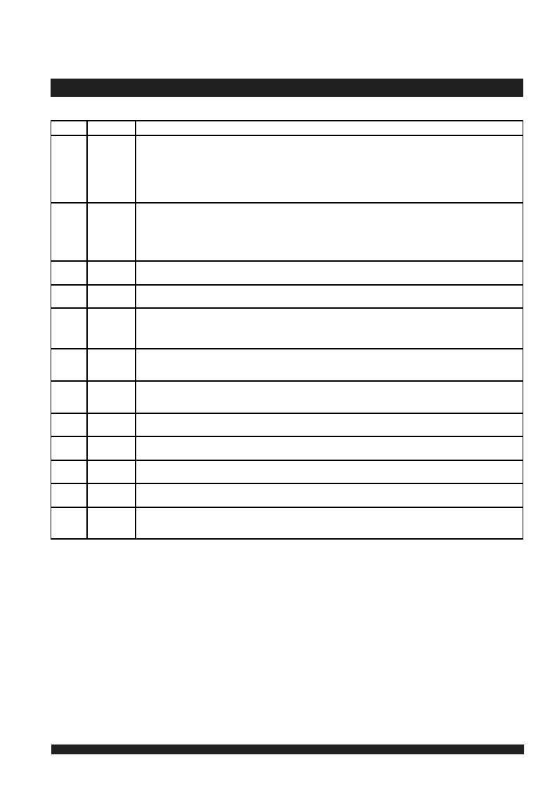
Pin Definitions
Symbol
Pin Function
Description
DQ[X:0]
Input/Output
Synchronous
Data I/O signals. Data inputs are sampled on the rising edge of K and
K
during valid write operations. Data outputs are driven during a
valid read operation. The outputs are aligned wth the rising edge of both C and
C
during normal operation. When operating in a single
clock mode (C and
C
tied high), the outputs are aligned with the rising edge of both K and
K
. When a Read operation is not initiated or
LD
is high (deselected) during the rising edge of K, DQ[X:O] are automatically driven to high impedance after any previous read
operation in progress completes.
1M x 18 -- DQ[17:0]
512K x 36 -- DQ[35:0]
BW
0
,
BW
1,
BW
2
,
BW
3
Input
Synchronous
Byte Write Select 0, 1, 2, and 3 are active LOW Sampled on the rising edge of the K and again on the rising edge of
K
clocks during
write operations. Used to select which byte is written into the device during the current portion of the write operations. Bytes not written
remain unaltered. All the byte writes are sampled on the same edge as the data. Deselecting a Byte Write Select wll cause the
corresponding byte of data to be ignored and not written in to the device.
1M x 18 --
BW
0
controls DQ[8:0] and
BW
1
controls DQ[17:9]
512K x 36 --
BW
0
controls DQ[8:0],
BW
1
controls DQ[17:9],
BW
2
controls DQ[26:18] and
BW
3
controls DQ[35:27]
SA
Input
Synchronous
Address Inputs. Addresses are sampled on the rising edge of K clock during active read or write operations.
SA
0
Input
Synchronous
Burst count address bit on x18 and x36 DDRll devices. This bit allows changing the burst order in read or write operations, or
addressing to the individual word of a burst. See page 9 for all possible burst sequences.
LD
Input
Synchronous
Load Control Logic: Sampled on the rising edge of K. If
LD
is low a two word burst read or write operation will initiate as designated by
the R/
W
input. If
LD
is high during the rising edge of K, operations in progress will complete, but newoperations wll not be initiated.
R
/W
Input
Synchronous
Read or Write Control Logic. If
LD
is low during the rising edge of K, the R
/W
indicates whether a new operation should be a read or
write. If R/
W
is high, a read operation wll be initiated, if R/
W
is low a write operation wll be initiated. If the
LD
input is high during the
rising edge of K, the R/
W
input wll be ignored.
C
Input Clock
Positive Output Clock Input. C is used in conjunction wth
C
to clock out the Read data fromthe device. C and
C
can be used together
to deskewthe flight times of various devices on the board back to the controller See application example for further details.
C
Input Clock
Negative Output Clock Input.
C
is used in conjunction wth C to clock out the Read data fromthe device. C and
C
can be used together
to deskewthe flight times of various devices on the board back to the controller See application example for further details.
K
Input Clock
Positive Input Clock. The rising edge of K is used to capture synchronous inputs to the device and to drive out data through DQ[X:0]
when in single clock mode. All accesses are initiated on the rising edge of K.
K
Input Clock
Negative Input Clock.
K
is used to capture synchronous inputs being presented to the device and to drive out data through DQ[X:0]
when in single clock mode.
CQ,
CQ
Output Clock
Synchronous Echo clock outputs. The rising edges of these outputs are tightly matched to the synchronous data outputs and can be
used as a data valid indication. These signals are free running and do not stop when the output data is three stated.
ZQ
Input
Output Impedance Matching Input. This input is used to tune the device outputs to the systemdata bus impedance. DQ[X:0] output
impedance is set to 0.2 x RQ, where RQ is a resistor connected between ZQ and ground. Alternately, this pin can be connected directly
to V
DDQ
, which enables the mnimumimpedance mode. This pin cannot be connected directly to GND or left unconnected.
6112 tbl 02a
相關(guān)PDF資料 |
PDF描述 |
|---|---|
| IDTIDT71P71604250BQ | 18Mb Pipelined DDR⑩II SRAM Burst of 2 |
| IDTIDT71P71804167BQ | 18Mb Pipelined DDR⑩II SRAM Burst of 2 |
| IDTIDT71P71804200BQ | 18Mb Pipelined DDR⑩II SRAM Burst of 2 |
| IDTIDT71P71804250BQ | 18Mb Pipelined DDR⑩II SRAM Burst of 2 |
| IDT71P73104 | 18Mb Pipelined DDR⑩II SRAM Burst of 4 |
相關(guān)代理商/技術(shù)參數(shù) |
參數(shù)描述 |
|---|---|
| IDTIDT71P71604250BQ | 制造商:IDT 制造商全稱:Integrated Device Technology 功能描述:18Mb Pipelined DDR⑩II SRAM Burst of 2 |
| IDTIDT71P71804167BQ | 制造商:IDT 制造商全稱:Integrated Device Technology 功能描述:18Mb Pipelined DDR⑩II SRAM Burst of 2 |
| IDTIDT71P71804200BQ | 制造商:IDT 制造商全稱:Integrated Device Technology 功能描述:18Mb Pipelined DDR⑩II SRAM Burst of 2 |
| IDTIDT71P71804250BQ | 制造商:IDT 制造商全稱:Integrated Device Technology 功能描述:18Mb Pipelined DDR⑩II SRAM Burst of 2 |
| IDTIDT71P79104167BQ | 制造商:IDT 制造商全稱:Integrated Device Technology 功能描述:18Mb Pipelined DDR⑩II SIO SRAM Burst of 2 |
發(fā)布緊急采購,3分鐘左右您將得到回復(fù)。