- 您現(xiàn)在的位置:買賣IC網(wǎng) > PDF目錄2002 > ISLA224S25IR1Z (Intersil)IC ADC PDF資料下載
參數(shù)資料
| 型號(hào): | ISLA224S25IR1Z |
| 廠商: | Intersil |
| 文件頁(yè)數(shù): | 1/38頁(yè) |
| 文件大小: | 0K |
| 描述: | IC ADC |
| 標(biāo)準(zhǔn)包裝: | 1 |
| 系列: | * |
當(dāng)前第1頁(yè)第2頁(yè)第3頁(yè)第4頁(yè)第5頁(yè)第6頁(yè)第7頁(yè)第8頁(yè)第9頁(yè)第10頁(yè)第11頁(yè)第12頁(yè)第13頁(yè)第14頁(yè)第15頁(yè)第16頁(yè)第17頁(yè)第18頁(yè)第19頁(yè)第20頁(yè)第21頁(yè)第22頁(yè)第23頁(yè)第24頁(yè)第25頁(yè)第26頁(yè)第27頁(yè)第28頁(yè)第29頁(yè)第30頁(yè)第31頁(yè)第32頁(yè)第33頁(yè)第34頁(yè)第35頁(yè)第36頁(yè)第37頁(yè)第38頁(yè)

1
CAUTION: These devices are sensitive to electrostatic discharge; follow proper IC Handling Procedures.
1-888-INTERSIL or 1-888-468-3774
| Copyright Intersil Americas LLC 2011-2013. All Rights Reserved
Intersil (and design) and FemtoCharge are trademarks owned by Intersil Corporation or one of its subsidiaries.
All other trademarks mentioned are the property of their respective owners.
Dual 14-Bit, 250/200/125 MSPS JESD204B High Speed
Serial Output ADC
ISLA224S
The ISLA224S is a series of low-power, high-performance,
dual-channel 14-bit, analog-to-digital converters. Designed
with FemtoCharge technology on a standard CMOS process,
the series supports sampling rates of up to 250MSPS. The
ISLA224S is part of a pin-compatible family of 12- and 14-bit
dual-channel A/Ds with maximum sample rates ranging from
125MSPS to 250MSPS and shares the same analog core as
Intersil's proven ISLA224P series of ADCs. The family
minimizes power consumption while providing state-of-the art
dynamic performance, offering an optimal performance-vs-
power trade-off.
Differentiating the ISLA224S from the ISLA224P is its highly
configurable, JESD204B-compliant, high speed serial output
link. The link offers data rates up to 4.375Gbps per lane and
multiple packing modes. It can be configured to use two or
three lanes to transmit the conversion data, allowing for
flexibility in the receiver design. The SERDES transmitter also
provides deterministic latency and multi-chip time alignment
support to satisfy an application's complex synchronization
requirements.
A serial peripheral interface (SPI) port allows for extensive
configurability of the JESD204B transmitter including access
to its built-in link and transport-layer test patterns. The SPI port
also provides control for numerous additional features
including the fine gain and offset adjustments of the two ADC
cores as well as the programmable clock divider, enabling 2x
and 4x harmonic clocking.
The ISLA224S is available in a space-saving 7mmx7mm 48 Ld
QFN package. The package features a thermal pad for
improved thermal performance and is specified over the full
industrial temperature range (-40°C to +85°C).
Features
JESD204A/B High Speed Data Interface
-JESD204A Compliant
- JESD204B Device Subclass 0 Compliant
- JESD204B Device Subclass 2 Compatible
- Up to 3 JESD204 Output Lanes Running up to 4.375Gbps
- Highly Configurable JESD204 Transmitter
Multiple Chip Time Alignment and Deterministic Latency
Support (JESD204B Device Subclass 2)
SPI Programmable Debugging Features and Test Patterns
48-pin QFN 7mmx7mm Package
Key Specifications
SNR @ 250/200/125MSPS
73.2/74.1/75.1 dBFS fIN = 30MHz
72.4/72.9/73.2 dBFS fIN = 190MHz
SFDR @ 250/200/125MSPS
82/91/94 dBc fIN = 30MHz
84/82/81 dBc fIN = 190MHz
Total Power Consumption: 989mW @ 250MSPS
Applications
Radar and Satellite Antenna Array Processing
Broadband Communications and Microwave Receivers
High-Performance Data Acquisition
Communications Test Equipment
High-Speed Medical Imaging
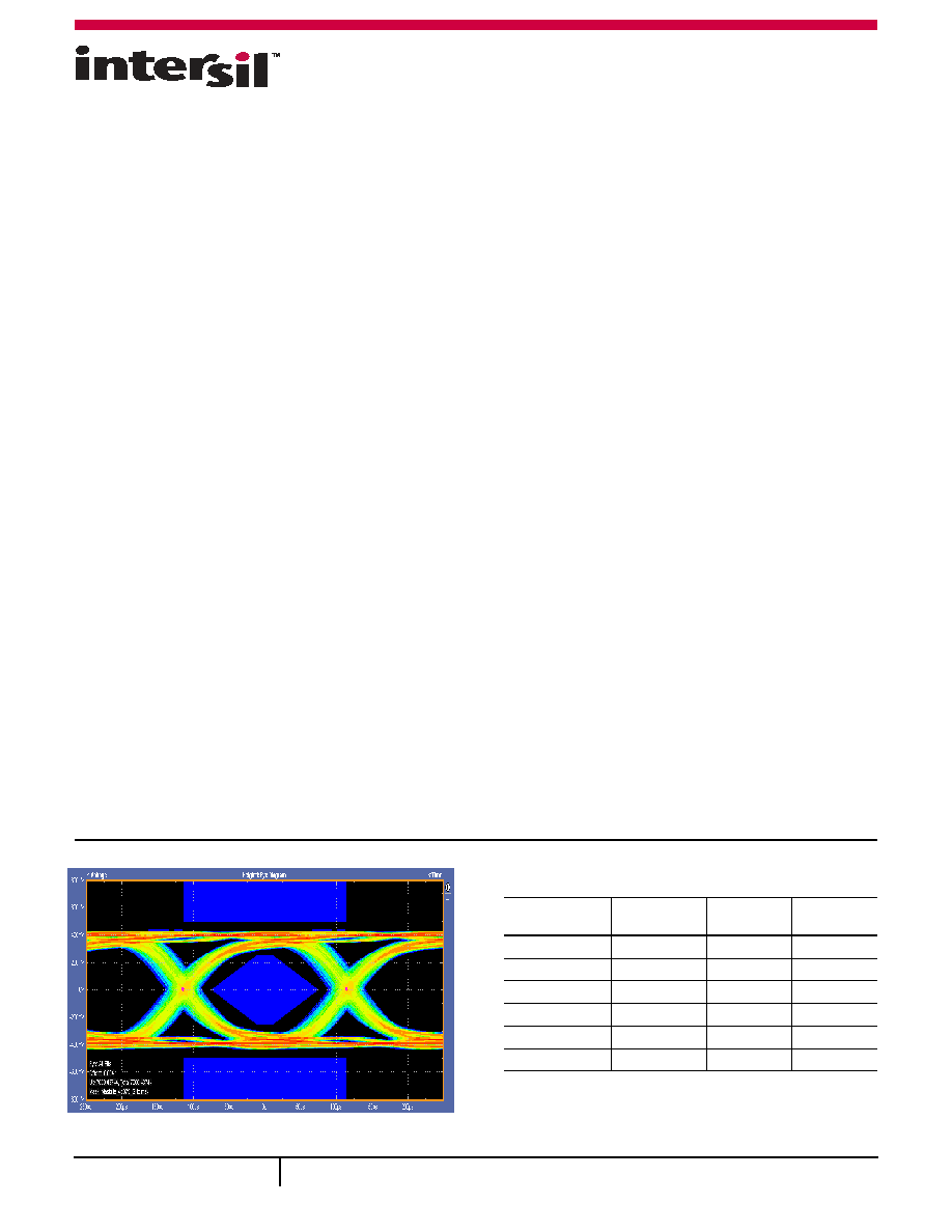
FIGURE 1. SERDES DATA EYE AT 4.375Gbps
Pin-Compatible Family
MODEL
RESOLUTION
SPEED
(MSPS)
PRODUCT
AVAILABILITY
ISLA224S25
14
250
Now
ISLA224S20
14
200
Now
ISLA224S12
14
125
Now
ISLA222S25
12
250
Now
ISLA222S20
12
200
Now
ISLA222S12
12
125
Now
April 25, 2013
FN7911.2
相關(guān)PDF資料 |
PDF描述 |
|---|---|
| KAD2708C-27Q68 | IC ADC 8BIT 275MSPS PAR 68-QFN |
| KAD2708L-27Q68 | IC ADC 8BIT 275MSPS PAR 68-QFN |
| KAD2710C-27Q68 | IC ADC 10BIT 275MSPS PAR 68-QFN |
| KAD2710L-21Q68 | IC ADC 10BIT 210MSPS SGL 68-QFN |
| KAD5510P-25Q48 | IC ADC 10BIT CMOS 250MSPS 48QFN |
相關(guān)代理商/技術(shù)參數(shù) |
參數(shù)描述 |
|---|---|
| ISLA224S25IR48EV1Z | 制造商:INTERSIL 制造商全稱:Intersil Corporation 功能描述:Dual 12-Bit, 250/200/125 MSPS JESD204B High Speed Serial Output ADC |
| ISLEM-BDGSTKEV1Z | 制造商:Intersil Corporation 功能描述:DAQ ON A STICK, E-MICRO STRAIN GAUGE, EVAL BOARD 1, ROHS COM - Bulk 制造商:Intersil Corporation 功能描述:EVAL BOARD FOR STRAIN GAUGE |
| ISLI2C-KIT | 制造商:Intersil Corporation 功能描述:ISLI2C - USB INTERFACE - Bulk |
| ISLN312AD3ST | 制造商:Fairchild Semiconductor Corporation 功能描述: |
| ISLT1102 | 制造商:ISOCOM 制造商全稱:ISOCOM 功能描述:ISLT1102 ( Long Creepage ) |
發(fā)布緊急采購(gòu),3分鐘左右您將得到回復(fù)。