- 您現(xiàn)在的位置:買(mǎi)賣(mài)IC網(wǎng) > PDF目錄383200 > IXLD02SI (IXYS Corporation) Differential 2A Ultra Fast Laser Diode Driver PDF資料下載
參數(shù)資料
| 型號(hào): | IXLD02SI |
| 廠商: | IXYS Corporation |
| 英文描述: | Differential 2A Ultra Fast Laser Diode Driver |
| 中文描述: | 差分甲超快速激光二極管驅(qū)動(dòng)器 |
| 文件頁(yè)數(shù): | 2/6頁(yè) |
| 文件大小: | 171K |
| 代理商: | IXLD02SI |
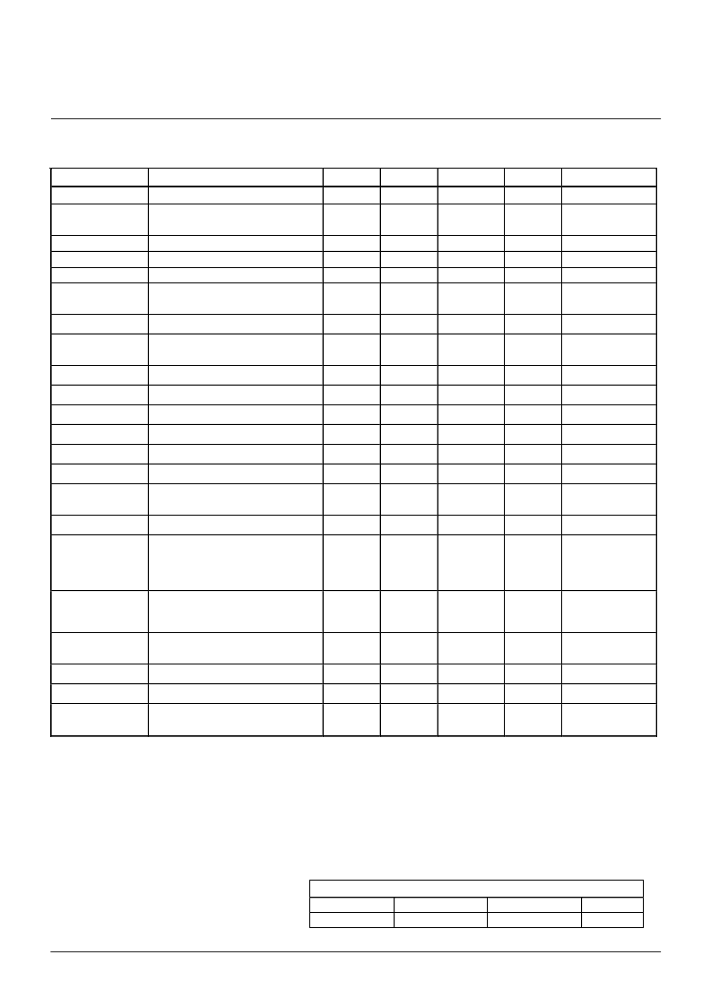
2
IXLD02SI
Absolute Maximum Ratings
(Note 1)
Name
VDD
Definition
Min
-0.4
Typ
Max
5.5
Units
V
Test Conditions
Logic supply input voltage
VDDA
Analog bias supply input voltage
-0.4
5.5
V
VTT
IBI
V
IBI
Internal bias voltage input
Internal bias current input
Applied IBI terminal voltage
Pulse width programming
current input
Applied IPW terminal voltage
Output current programming
input
Applied IOP terminal voltage
-0.4
-10
-0.4
VDDA/2
0.1
VDDA+.5
10
VDDin+0.5
V
mA
V
IPW
-10
0.1
10
mA
V
IPW
-0.4
VDDin+0.5
V
IOP
-10
1
10
mA
V
IOP
V
PDN
V
RST
V
FIN
V
OUT
V
OUT
-0.4
VDDin+0.5
V
Power-down logic input
-0.4
VDDin+0.5
V
Reset logic input
-0.4
VDDin+0.5
V
Pulse frequency logic input
-0.4
V
Pulse current true output
-0.1
3
Amps
OUT terminal voltage
Pulse current complement
output
OUTB terminal voltage
-0.4
9
V
OUTB
-0.1
3
Amps
V
OUTB
-0.4
9
V
T
C
Device Case Temperature
-40
25
85
o
C
Measured at the
bottom of the
SO28 package
heat slug insert.
SO28 package
heat slug insert
held at T
C
=85
o
C.
P
D
Package power dissipation @
T
C
=85C
32
Watts
R
THJC
Thermal resistance, junction to
case
Junction Temperature
2
o
C/W
T
J
T
S
150
o
C
Storage temperature
Lead temperature (soldering, 10
sec)
-55
150
o
C
T
L
300
o
C
Note 1:
Operating the device beyond parameters with listed “Absolute Maximum Ratings” may cause permanent
damage to the device. Typical values indicate conditions for which the device is intended to be functional, but do not
guarantee specific performance limits. The guaranteed specifications apply only for the test conditions listed.
Exposure to absolute maximum rated conditions for extended periods may affect device reliability.
CAUTION: These devices are sensitive to electrostatic discharge; follow proper ESD procedures
when handling and assembling this component.
Ordering Information
Part Number Package Type Temp. Range
IXLD02SI
28-Pin SOIC
Grade
-40
°
C to +85
°
C Industrial
相關(guān)PDF資料 |
PDF描述 |
|---|---|
| IXLF19N250A | High Voltage IGBT |
| IXR100 | Isolated, Self-Powered,Temperature Sensor Conditioning 4-20mA Two-Wire Transmitter(隔離的,自備電源的溫度傳感器4-20mA可兩線傳輸) |
| IXRH50N100 | IGBT with Reverse Blocking capability |
| IXRH50N120 | IGBT with Reverse Blocking capability |
| IXRH50N60 | IGBT with Reverse Blocking capability |
相關(guān)代理商/技術(shù)參數(shù) |
參數(shù)描述 |
|---|---|
| IXLD1426COA | 制造商:未知廠家 制造商全稱:未知廠家 功能描述:Dual MOSFET Driver |
| IXLD1426CPA | 制造商:未知廠家 制造商全稱:未知廠家 功能描述:Dual MOSFET Driver |
| IXLD1427COA | 制造商:未知廠家 制造商全稱:未知廠家 功能描述:Dual MOSFET Driver |
| IXLD1427CPA | 制造商:未知廠家 制造商全稱:未知廠家 功能描述:Dual MOSFET Driver |
| IXLD1428CPA | 制造商:未知廠家 制造商全稱:未知廠家 功能描述:Dual MOSFET Driver |
發(fā)布緊急采購(gòu),3分鐘左右您將得到回復(fù)。