- 您現(xiàn)在的位置:買賣IC網(wǎng) > PDF目錄373069 > K4T1G164QD (SAMSUNG SEMICONDUCTOR CO. LTD.) 1Gb D-die DDR2 SDRAM Specification PDF資料下載
參數(shù)資料
| 型號(hào): | K4T1G164QD |
| 廠商: | SAMSUNG SEMICONDUCTOR CO. LTD. |
| 英文描述: | 1Gb D-die DDR2 SDRAM Specification |
| 中文描述: | 1Gb的?芯片DDR2內(nèi)存規(guī)格 |
| 文件頁數(shù): | 27/27頁 |
| 文件大小: | 589K |
| 代理商: | K4T1G164QD |
第1頁第2頁第3頁第4頁第5頁第6頁第7頁第8頁第9頁第10頁第11頁第12頁第13頁第14頁第15頁第16頁第17頁第18頁第19頁第20頁第21頁第22頁第23頁第24頁第25頁第26頁當(dāng)前第27頁
K4T1G084QD
K4T1G164QD
Rev. 1.0 March 2007
DDR2 SDRAM
25 of 29
tDS
V
DDQ
V
IH(ac)
min
V
IH(dc)
min
V
REF(dc)
V
IL(dc)
max
V
IL(ac)
max
V
SS
DQS
DQS
tDH
tDS
tDH
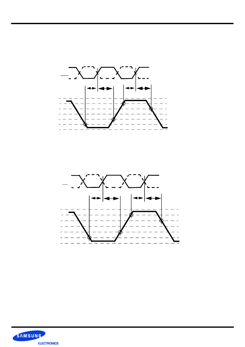
31. Input waveform timing is referenced from the input signal crossing at the V
IH(ac)
level for a rising signal and V
IL(ac)
for a falling signal applied to the
device under test.
32. Input waveform timing is referenced from the input signal crossing at the V
IL(dc)
level for a rising signal and V
IH(dc)
for a falling signal applied to the
device under test.
33. tWTR is at lease two clocks (2 * tCK) independent of operation frequency.
34. Input waveform timing with single-ended data strobe enabled MR[bit10] = 1, is referenced from the input signal crossing at the VIH(ac) level to the
single-ended data strobe crossing VIH/L(dc) at the start of its transition for a rising signal, and from the input signal crossing at the VIL(ac) level to the
single-ended data strobe crossing VIH/L(dc) at the start of its transition for a falling signal applied to the device under test. The DQS signal must be
monotonic between Vil(dc)max and Vih(dc)min.
35. Input waveform timing with single-ended data strobe enabled MR[bit10] = 1, is referenced from the input signal crossing at the VIH(dc) level to the
single-ended data strobe crossing VIH/L(ac) at the end of its transition for a rising signal, and from the input signal crossing at the VIL(dc) level to the
single-ended data strobe crossing VIH/L(ac) at the end of its transition for a falling signal applied to the device under test. The DQS signal must be
monotonic between Vil(dc)max and Vih(dc)min.
36. tCKEmin of 3 clocks means CKE must be registered on three consecutive positive clock edges. CKE must remain at the valid input level the entire
time it takes to achieve the 3 clocks of registeration. Thus, after any cKE transition, CKE may not transitioin from its valid level during the time period
of tIS + 2*tCK + tIH.
tIS
V
DDQ
V
IH(ac)
min
V
IH(dc)
min
V
REF(dc)
V
IL(dc)
max
V
IL(ac)
max
V
SS
CK
CK
tIH
tIS
tIH
29. Input waveform timing with differential data strobe enabled MR[bit10]=0, is referenced from the input signal crossing at the V
IH(ac)
level to the differen-
tial data strobe crosspoint for a rising signal, and from the input signal crossing at the V
IL(ac)
level to the differential data strobe crosspoint for a falling
signal applied to the device under test.
30. Input waveform timing with differential data strobe enabled MR[bit10]=0, is referenced from the input signal crossing at the V
IH(dc)
level to the differen-
tial data strobe crosspoint for a rising signal and V
IL(dc)
to the differential data strobe crosspoint for a falling signal applied to the device under test.
< Differential Input waveform timing >
相關(guān)PDF資料 |
PDF描述 |
|---|---|
| K4T1G084QQ-HC(L)F7 | 1Gb Q-die DDR2 SDRAM Specification |
| K4T1G044QQ | 1Gb Q-die DDR2 SDRAM Specification |
| K4T1G044QQ-HC(L)E6 | 1Gb Q-die DDR2 SDRAM Specification |
| K4T1G044QQ-HC(L)E7 | 1Gb Q-die DDR2 SDRAM Specification |
| K4T1G044QQ-HC(L)F7 | 1Gb Q-die DDR2 SDRAM Specification |
相關(guān)代理商/技術(shù)參數(shù) |
參數(shù)描述 |
|---|---|
| K4T1G164QD-ZCE6000 | 制造商:Samsung Semiconductor 功能描述: |
| K4T1G164QE | 制造商:SAMSUNG 制造商全稱:Samsung semiconductor 功能描述:Consumer Memory |
| K4T1G164QE-HCE7000 | 制造商:SAMSUNG 制造商全稱:Samsung semiconductor 功能描述:1Gb E-die DDR2 SDRAM 60FBGA/84FBGA with Lead-Free & Halogen-Free (RoHS compliant) |
| K4T1G164QE-HCLE6 | 制造商:SAMSUNG 制造商全稱:Samsung semiconductor 功能描述:1Gb E-die DDR2 SDRAM |
| K4T1G164QE-HCLE7 | 制造商:SAMSUNG 制造商全稱:Samsung semiconductor 功能描述:1Gb E-die DDR2 SDRAM |
發(fā)布緊急采購,3分鐘左右您將得到回復(fù)。