- 您現(xiàn)在的位置:買賣IC網(wǎng) > PDF目錄373088 > K9F6408U0C (SAMSUNG SEMICONDUCTOR CO. LTD.) 8M x 8 Bit NAND Flash Memory PDF資料下載
參數(shù)資料
| 型號(hào): | K9F6408U0C |
| 廠商: | SAMSUNG SEMICONDUCTOR CO. LTD. |
| 英文描述: | 8M x 8 Bit NAND Flash Memory |
| 中文描述: | 8米× 8位NAND閃存 |
| 文件頁(yè)數(shù): | 3/30頁(yè) |
| 文件大小: | 784K |
| 代理商: | K9F6408U0C |
第1頁(yè)第2頁(yè)當(dāng)前第3頁(yè)第4頁(yè)第5頁(yè)第6頁(yè)第7頁(yè)第8頁(yè)第9頁(yè)第10頁(yè)第11頁(yè)第12頁(yè)第13頁(yè)第14頁(yè)第15頁(yè)第16頁(yè)第17頁(yè)第18頁(yè)第19頁(yè)第20頁(yè)第21頁(yè)第22頁(yè)第23頁(yè)第24頁(yè)第25頁(yè)第26頁(yè)第27頁(yè)第28頁(yè)第29頁(yè)第30頁(yè)
FLASH MEMORY
3
K9F6408U0C
GENERAL DESCRIPTION
The K9F6408U0C is a 8M(8,388,608)x8bit NAND Flash Memory with a spare 256K(262,144)x8bit. The device is offered in 3.3V Vcc.
Its NAND cell provides the most cost-effective solution for the solid state mass storage market. A program operation programs the
528-byte page in typical 200
μ
s and an erase operation can be performed in typical 2ms on an 8K-byte block. Data in the page can be
read out at 50ns cycle time per byte. The I/O pins serve as the ports for address and data input/output as well as command inputs.
The on-chip write controller automates all program and erase functions including pulse repetition, where required, and internal verifi-
cation and margining of data. Even the write-intensive systems can take advantage of the K9F6408U0C
′
s extended reliability of 100K
program/erase cycles by providing ECC(Error Correcting Code) with real time mapping-out algorithm. These algorithms have been
implemented in many mass storage applications and also the spare 16 bytes of a page combined with the other 512 bytes can be uti-
lized by system-level ECC. The K9F6408U0C is an optimum solution for large nonvolatile storage applications such as solid state file
storage, digital voice recorder, digital still camera and other portable applications requiring non-volatility.
FEATURES
Voltage Supply
- 1.70~1.95V
Organization
- Memory Cell Array : (8M + 256K)bit x 8bit
- Data Register : (512 + 16)bit x8bit
Automatic Program and Erase
- Page Program : (512 + 16)Byte
- Block Erase : (8K + 256)Byte
528-Byte Page Read Operation
- Random Access : 10
μ
s(Max.)
- Serial Page Access
- 50ns
Fast Write Cycle Time
- Program Time : 200
μ
s(Typ.)
- Block Erase Time : 2ms(Typ.)
8M x 8 Bit Bit NAND Flash Memory
Command/Address/Data Multiplexed I/O Port
Hardware Data Protection
- Program/Erase Lockout During Power Transitions
Reliable CMOS Floating-Gate Technology
- Endurance : 100K Program/Erase Cycles
- Data Retention : 10 Years
Command Register Operation
Package
- K9F6408U0C-TCB0/TIB0
44(40) - Lead TSOP Type II (400mil / 0.8 mm pitch)
- K9F6408U0C-BCB0/BIB0
48 - Ball TBGA ( 6 x 8.5 /0.8mm pitch , Width 1.0 mm)
- K9F6408U0C-VCB0/VIB0
48 - Pin WSOP I (12X17X0.7mm)
- K9F6408U0C-QCB0/QIB0 : Pb-free Package
44(40) - Lead TSOP Type II (400mil / 0.8 mm pitch)
- K9F6408U0C-HCB0/HIB0 : Pb-free Package
48 - Ball TBGA ( 6 x 8.5 /0.8mm pitch , Width 1.0 mm)
- K9F6408U0C-FCB0/FIB0 : Pb-free Package
48 - Pin WSOP I (12X17X0.7mm)
* K9F6408U0C-V,F(WSOPI ) is the same device as
K9F6408U0C-T,Q(TSOPII) except package type.
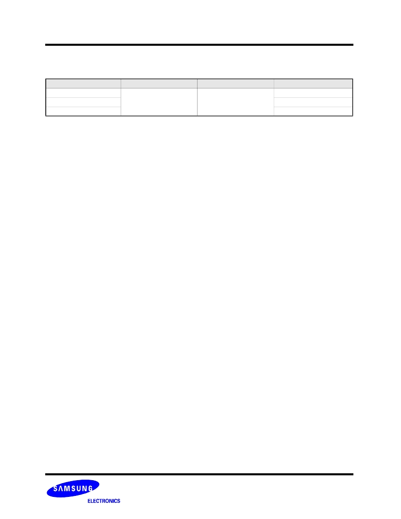
PRODUCT LIST
Part Number
Vcc Range
Organization
PKG Type
K9F6408U0C-B,H
2.7 ~ 3.6V
X8
TBGA
K9F6408U0C-T,Q
TSOP II
K9F6408U0C-V,F
WSOP I
相關(guān)PDF資料 |
PDF描述 |
|---|---|
| K9K1208D0C | TV 37C 37#16 SKT RECP |
| K9K1216Q0C | SCSI 2 MALE-MALE 3 FT |
| K9K1216U0C | M1 - DVI-D W/USB 10 FEET |
| K9K1216D0C | 64M x 8 Bit , 32M x 16 Bit NAND Flash Memory |
| K9K1208Q0C | 64M x 8 Bit , 32M x 16 Bit NAND Flash Memory |
相關(guān)代理商/技術(shù)參數(shù) |
參數(shù)描述 |
|---|---|
| K9F6408U0C-B | 制造商:SAMSUNG 制造商全稱:Samsung semiconductor 功能描述:8M x 8 Bit Bit NAND Flash Memory |
| K9F6408U0C-F | 制造商:SAMSUNG 制造商全稱:Samsung semiconductor 功能描述:8M x 8 Bit NAND Flash Memory |
| K9F6408U0C-H | 制造商:SAMSUNG 制造商全稱:Samsung semiconductor 功能描述:8M x 8 Bit Bit NAND Flash Memory |
| K9F6408U0C-Q | 制造商:SAMSUNG 制造商全稱:Samsung semiconductor 功能描述:8M x 8 Bit NAND Flash Memory |
| K9F6408U0C-T | 制造商:SAMSUNG 制造商全稱:Samsung semiconductor 功能描述:8M x 8 Bit Bit NAND Flash Memory |
發(fā)布緊急采購(gòu),3分鐘左右您將得到回復(fù)。