- 您現(xiàn)在的位置:買賣IC網(wǎng) > PDF目錄373088 > K9K1G08U0A (SAMSUNG SEMICONDUCTOR CO. LTD.) 128M x 8 Bit / 64M x 16 Bit NAND Flash Memory PDF資料下載
參數(shù)資料
| 型號: | K9K1G08U0A |
| 廠商: | SAMSUNG SEMICONDUCTOR CO. LTD. |
| 英文描述: | 128M x 8 Bit / 64M x 16 Bit NAND Flash Memory |
| 中文描述: | 128M的× 8位/ 64米× 16位NAND閃存 |
| 文件頁數(shù): | 36/43頁 |
| 文件大小: | 906K |
| 代理商: | K9K1G08U0A |
第1頁第2頁第3頁第4頁第5頁第6頁第7頁第8頁第9頁第10頁第11頁第12頁第13頁第14頁第15頁第16頁第17頁第18頁第19頁第20頁第21頁第22頁第23頁第24頁第25頁第26頁第27頁第28頁第29頁第30頁第31頁第32頁第33頁第34頁第35頁當(dāng)前第36頁第37頁第38頁第39頁第40頁第41頁第42頁第43頁
FLASH MEMORY
36
K9K1G08U0A
K9K1G08Q0A
K9K1G16U0A
K9K1G16Q0A
Preliminary
Copy-Back Program
The copy-back program is configured to quickly and efficiently rewrite data stored in one page within the plane to another page within
the same plane without utilizing an external memory. Since the time-consuming sequently-reading and its re-loading cycles are
removed, the system performance is improved. The benefit is especially obvious when a portion of a block is updated and the rest of
the block also need to be copied to the newly assigned free block. The operation for performing a copy-back program is a sequential
execution of page-read without burst-reading cycle and copying-program with the address of destination page. A normal read opera-
tion with "00h" command and the address of the source page moves the whole 528byte data into the internal buffer. As soon as the
device returns to Ready state, Page-Copy Data-input command (8Ah) with the address cycles of destination page followed may be
written. The Program Confirm command (10h) is required to actually begin the programming operation. Copy-Back Program opera-
tion is allowed only within the same memory plane. Once the Copy-Back Program is finished, any additional partial page program-
ming into the copied pages is prohibited before erase. A14, A15 and A26 must be the same between source and target page.
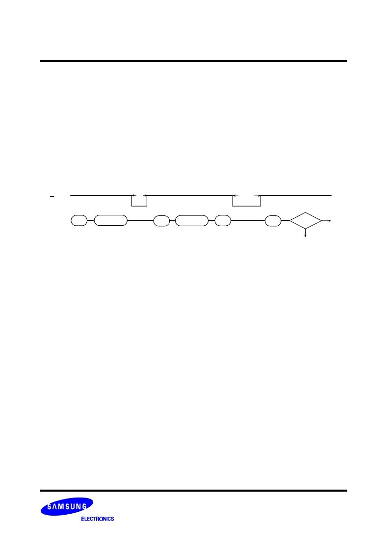
Figure20 shows the command sequence for single plane operation.
"When there is a program-failure at Copy-Back operation,
error is reported by pass/fail status. But, if Copy-Back operations are accumulated over time, bit error due to charge loss is
not checked by external error detection/correction scheme. For this reason, two bit error correction is recommended for the
use of Copy-Back operation."
Figure 20. One Page Copy-Back program Operation
00h
A
0
~ A
7
& A
9
~ A
26
Source Address
I/O
0
~
7
R/B
Add.(4Cycles)
I/O
0
Pass
8Ah
70h
Fail
t
PROG
A
0
~ A
7
& A
9
~ A
26
Destination Address
Add.(4Cycles)
t
R
10h
相關(guān)PDF資料 |
PDF描述 |
|---|---|
| K9K1G08U0A1 | 128M x 8 Bit / 64M x 16 Bit NAND Flash Memory |
| K9K1G16Q0A | 128M x 8 Bit / 64M x 16 Bit NAND Flash Memory |
| K9K1G16U0A | 128M x 8 Bit / 64M x 16 Bit NAND Flash Memory |
| K9K2G08U1A | 128M x 8 Bit / 256M x 8 Bit NAND Flash Memory |
| K9F1G08R0A | Circular Connector; MIL SPEC:MIL-DTL-38999 Series III; Body Material:Metal; Series:TVP00; No. of Contacts:99; Connector Shell Size:25; Connecting Termination:Crimp; Circular Shell Style:Wall Mount Receptacle; Body Style:Straight |
相關(guān)代理商/技術(shù)參數(shù) |
參數(shù)描述 |
|---|---|
| K9K1G08U0A1 | 制造商:SAMSUNG 制造商全稱:Samsung semiconductor 功能描述:128M x 8 Bit / 64M x 16 Bit NAND Flash Memory |
| K9K1G08U0B | 制造商:SAMSUNG 制造商全稱:Samsung semiconductor 功能描述:128M x 8 Bit NAND Flash Memory |
| K9K1G08U0B-JIB0000 | 制造商:Samsung Semiconductor 功能描述:1GB SLC DIE STACK X8 FBGA - Trays |
| K9K1G08U0M | 制造商:SAMSUNG 制造商全稱:Samsung semiconductor 功能描述:nand flash |
| K9K1G08U0M-YCB0 | 制造商:SAMSUNG 制造商全稱:Samsung semiconductor 功能描述:nand flash |
發(fā)布緊急采購,3分鐘左右您將得到回復(fù)。