- 您現(xiàn)在的位置:買賣IC網(wǎng) > PDF目錄373130 > KFG1G16D2M-DID6 (SAMSUNG SEMICONDUCTOR CO. LTD.) FLASH MEMORY(54MHz) PDF資料下載
參數(shù)資料
| 型號: | KFG1G16D2M-DID6 |
| 廠商: | SAMSUNG SEMICONDUCTOR CO. LTD. |
| 英文描述: | FLASH MEMORY(54MHz) |
| 中文描述: | 閃存(54MHz之間) |
| 文件頁數(shù): | 58/93頁 |
| 文件大?。?/td> | 1219K |
| 代理商: | KFG1G16D2M-DID6 |
第1頁第2頁第3頁第4頁第5頁第6頁第7頁第8頁第9頁第10頁第11頁第12頁第13頁第14頁第15頁第16頁第17頁第18頁第19頁第20頁第21頁第22頁第23頁第24頁第25頁第26頁第27頁第28頁第29頁第30頁第31頁第32頁第33頁第34頁第35頁第36頁第37頁第38頁第39頁第40頁第41頁第42頁第43頁第44頁第45頁第46頁第47頁第48頁第49頁第50頁第51頁第52頁第53頁第54頁第55頁第56頁第57頁當(dāng)前第58頁第59頁第60頁第61頁第62頁第63頁第64頁第65頁第66頁第67頁第68頁第69頁第70頁第71頁第72頁第73頁第74頁第75頁第76頁第77頁第78頁第79頁第80頁第81頁第82頁第83頁第84頁第85頁第86頁第87頁第88頁第89頁第90頁第91頁第92頁第93頁
OneNAND512/OneNAND1GDDP
FLASH MEMORY
58
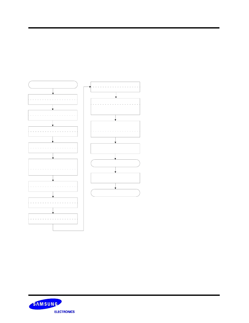
Figure 19. OTP load operation flow-chart
Note 1) FBA(NAND Flash Block Address) could be omitted or any address.
OTP Load(OTP Access+Load NAND)
OTP area is separated from NAND Flash Array, so it is accessed by OTP Access command instead of FBA. The content of OTP
could be loaded with the same sequence as normal load operation after being accessed by the command. If user wants to exit from
OTP access mode, Cold, Warm, Hot or NAND Flash Core Reset operation should be done.
* DBS, DFS is for DDP
Start
Wait for INT register
low to high transition
Add: F241h DQ[15]=INT
Write ’FPA, FSA’ of Flash
1)
Add: F107h DQ=FPA, FSA
OTP Load completed
Write ’Load’ Command
Add: F220h
DQ=0000h or 0013h
Wait for INT register
low to high transition
Add: F241h DQ[15]=INT
Write ’OTP Access’ Command
Add: F220h DQ=0075h
Write ’BSA, BSC’ of DataRAM
Add: F200h DQ=BSA, BSC
OTP Exit
Host reads data from
DataRAM
Do Cold/Warm/Hot
/NAND Flash Core Reset
Write ’DFS*, FBA’ of Flash
1)
Add: F100h DQ=DFS*’, FBA
Select DataRAM for DDP
Add: F101h DQ=DBS
Write 0 to interrupt register
Add: F241h DQ=0000h
Write 0 to interrupt register
Add: F241h DQ=0000h
Write ’OTP Access’ Command
Add: F220h DQ=0065h
相關(guān)PDF資料 |
PDF描述 |
|---|---|
| KFH1G16Q2M-DIB5 | FLASH MEMORY(54MHz) |
| KFG1G16D2M-DIB5 | FLASH MEMORY(54MHz) |
| KFH1G16D2M-DIB5 | FLASH MEMORY(54MHz) |
| KFG1216U2M | FLASH MEMORY |
| KFG1216U2M-DIB | FLASH MEMORY |
相關(guān)代理商/技術(shù)參數(shù) |
參數(shù)描述 |
|---|---|
| KFG1G16Q2A-DEB5000 | 制造商:Samsung Semiconductor 功能描述: |
| KFG1G16Q2A-DEB6000 | 制造商:Samsung Semiconductor 功能描述: |
| KFG1G16Q2A-DEB8000 | 制造商:Samsung Semiconductor 功能描述:1GNOFLASHADE-MUXED SLC W/X1663 FBGA(10X13) - Bulk |
| KFG1G16Q2B-DEB8000 | 制造商:Samsung SDI 功能描述:NAND Flash Serial 1.8V 1Gbit 64M x 16bit 8ns 63-Pin FBGA Tray |
| KFG1G16Q2C-AEB8000 | 制造商:Samsung Semiconductor 功能描述: |
發(fā)布緊急采購,3分鐘左右您將得到回復(fù)。