- 您現(xiàn)在的位置:買賣IC網(wǎng) > PDF目錄373129 > KFG2816D1M-DID (SAMSUNG SEMICONDUCTOR CO. LTD.) OneNAND SPECIFICATION PDF資料下載
參數(shù)資料
| 型號: | KFG2816D1M-DID |
| 廠商: | SAMSUNG SEMICONDUCTOR CO. LTD. |
| 英文描述: | OneNAND SPECIFICATION |
| 中文描述: | OneNAND的規(guī)格 |
| 文件頁數(shù): | 49/87頁 |
| 文件大小: | 1175K |
| 代理商: | KFG2816D1M-DID |
第1頁第2頁第3頁第4頁第5頁第6頁第7頁第8頁第9頁第10頁第11頁第12頁第13頁第14頁第15頁第16頁第17頁第18頁第19頁第20頁第21頁第22頁第23頁第24頁第25頁第26頁第27頁第28頁第29頁第30頁第31頁第32頁第33頁第34頁第35頁第36頁第37頁第38頁第39頁第40頁第41頁第42頁第43頁第44頁第45頁第46頁第47頁第48頁當前第49頁第50頁第51頁第52頁第53頁第54頁第55頁第56頁第57頁第58頁第59頁第60頁第61頁第62頁第63頁第64頁第65頁第66頁第67頁第68頁第69頁第70頁第71頁第72頁第73頁第74頁第75頁第76頁第77頁第78頁第79頁第80頁第81頁第82頁第83頁第84頁第85頁第86頁第87頁
OneNAND128
FLASH MEMORY
49
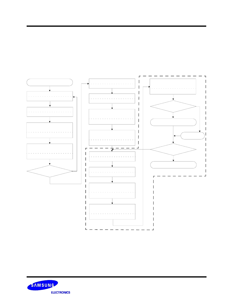
Multi Block Erase and Multi Block Erase Verify Read Operation
The device can be simultaneously erased in multi blocks unit, too. The block address of the memory location and Multi Block Erase
command may be repeated for erasing multi blocks. The final block address and Block Erase command initiate the internal multi
block erase routine. During Multi Block Erase routine, if the command except Multi Block Erase command is written before Block
Erase command is issued, Multi Block Erase operation will be aborted. Erase Suspend command is allowed only when INT is Low
after Block Erase command is issued.
Pass/fail status of each block in Multi Block Erase operation can be read by writing each block address and Multi Block Erase Verify
Read command. But the information of the failed address has to be managed by the firmware. After Block Erase operation, the pass/
fail status can be read with Multi Block Erase Verify Read command, too.
Note that a reset during a erase operation will cause data corruption at the corresponding location.
Figure 18. Multi Block Erase operation flow-chart
NOTE:
1. If there are the locked blocks in the specified range, the operation works as the follows.
Case 1. [BA(1)+0095h] + [BA(2, locked)+0095h] + ... + [BA(N-1)+0095h] + [BA(N)+0094h] = All specified blocks except BA(2) are erased.
Case 2. [BA(1)+0095h] + [BA(2)+0095h] + ... + [BA(N-1)+0095h] + [BA(N, locked)+0094h] = If the last command, Block Erase command, is put
together with the locked block address, Multi Block Erase operation doesn’t start and is suspended until right command and address input.
Case 3. [BA(1)+0095h] + [BA(2)+0095h] + ... + [BA(N-1)+0095h] + [BA(N, locked)+0094h] + [BA(N+1)+0094h]= All specified blocks except BA(N) are
erased.
2. The OnGo bit of Controller Status register is set to ’1’(busy) from the time of writing the 1st block address to be latched until the actual erase has fin-
ished.
3. Even though the failed blocked happen during multi block erase operation, the device continues the erase operation until other specified blocks are
erased.
Start
Write ’FBA’ of Flash
Add: F100h DQ=FBA
Write ’Multi Block Erase’
Command
Add: F220h DQ=0095h
Wait for INT register
low to high transition
Add: F241h DQ=[15]=INT
Final Multi Block
Erase
YES
NO
Write 0 to interrupt register
Add: F241h DQ=0000h
Write ’FBA’ of Flash
Add: F100h DQ=FBA
Write ’Block Erase
Command’
Add: F220h DQ=0094h
Wait for INT register
low to high transition
Add: F241h DQ=[15]=INT
Write 0 to interrupt register
Add: F241h DQ=0000h
Multi Block Erase Verify Read
Write ’FBA’ of Flash
Add: F100h DQ=FBA
Write ’Multi Block Erase
Verify Read Command’
Add: F220h DQ=0071h
Wait for INT register
low to high transition
Add: F241h DQ=[15]=INT
Write 0 to interrupt register
Add: F241h DQ=0000h
Read Controller
Status Register
Add: F240h DQ[10]=Error
DQ[10]=0
Multi Block Erase completed
Final Multi Block
Erase Address
YES
NO
Erase completed
YES
Erase Error
NO
相關(guān)PDF資料 |
PDF描述 |
|---|---|
| KFG2816D1M-PEB | OneNAND SPECIFICATION |
| KFG2816D1M-PED | OneNAND SPECIFICATION |
| KFG2816D1M-PIB | OneNAND SPECIFICATION |
| KFH1G16D2M-DEB | FLASH MEMORY |
| KFG1216U2M-DEB | FLASH MEMORY |
相關(guān)代理商/技術(shù)參數(shù) |
參數(shù)描述 |
|---|---|
| KFG2816D1M-PEB | 制造商:SAMSUNG 制造商全稱:Samsung semiconductor 功能描述:OneNAND SPECIFICATION |
| KFG2816D1M-PED | 制造商:SAMSUNG 制造商全稱:Samsung semiconductor 功能描述:OneNAND SPECIFICATION |
| KFG2816D1M-PIB | 制造商:SAMSUNG 制造商全稱:Samsung semiconductor 功能描述:OneNAND SPECIFICATION |
| KFG2816D1M-PID | 制造商:SAMSUNG 制造商全稱:Samsung semiconductor 功能描述:OneNAND SPECIFICATION |
| KFG2816Q1M | 制造商:SAMSUNG 制造商全稱:Samsung semiconductor 功能描述:OneNAND SPECIFICATION |
發(fā)布緊急采購,3分鐘左右您將得到回復。