- 您現(xiàn)在的位置:買賣IC網(wǎng) > PDF目錄373129 > KFG2816U1M-PEB (SAMSUNG SEMICONDUCTOR CO. LTD.) OneNAND SPECIFICATION PDF資料下載
參數(shù)資料
| 型號(hào): | KFG2816U1M-PEB |
| 廠商: | SAMSUNG SEMICONDUCTOR CO. LTD. |
| 英文描述: | OneNAND SPECIFICATION |
| 中文描述: | OneNAND的規(guī)格 |
| 文件頁數(shù): | 24/87頁 |
| 文件大小: | 1175K |
| 代理商: | KFG2816U1M-PEB |
第1頁第2頁第3頁第4頁第5頁第6頁第7頁第8頁第9頁第10頁第11頁第12頁第13頁第14頁第15頁第16頁第17頁第18頁第19頁第20頁第21頁第22頁第23頁當(dāng)前第24頁第25頁第26頁第27頁第28頁第29頁第30頁第31頁第32頁第33頁第34頁第35頁第36頁第37頁第38頁第39頁第40頁第41頁第42頁第43頁第44頁第45頁第46頁第47頁第48頁第49頁第50頁第51頁第52頁第53頁第54頁第55頁第56頁第57頁第58頁第59頁第60頁第61頁第62頁第63頁第64頁第65頁第66頁第67頁第68頁第69頁第70頁第71頁第72頁第73頁第74頁第75頁第76頁第77頁第78頁第79頁第80頁第81頁第82頁第83頁第84頁第85頁第86頁第87頁
OneNAND128
FLASH MEMORY
24
7.12 Start Address5 Register: F104h
: N/A
7.13 Start Address6 Register: F105h
: N/A
7.14 Start Address7 Register: F106h
: N/A
7.15 Start Address8 Register (R/W): F107h, default=0000h
FPA
(NAND Flash Page Address): NAND Flash start page address in a block for page read or copy back program or program operation.
FPA(default value)=000000
FPA range: 000000~111111 , 6bits for 64 pages
FSA
(Flash Sector Address): NAND Flash start sector address in a page for read or copy back program or program operation.
FSA(default value) = 0
FSA range : 0~1, 1bits for 2 sectors
15
14
13
12
11
10
9
8
7
6
5
4
3
2
1
0
Reserved (00000000)
FPA
Reserved
FSA
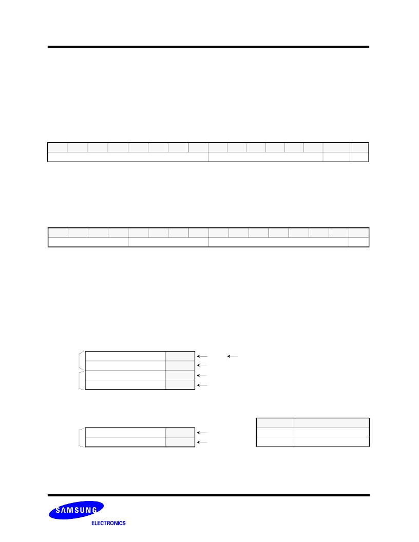
7.16 Start Buffer Register (R/W): F200h, default=0000h
BSC
(BufferRAM Sector Count): this field specifies the number of sectors to be read or programmed or copy back programmed.
Its maximum count is 2 sectors at 0(default value)value.
For a single sector access, it should be programmed as value 1 and it should be programmed as value 0 for two sectors.
However internal RAM buffer reached to 1 value(max. value), it counts up to 0 value to satisfy BSC value.
for example) if BSA=1101, BSC=0, then selected BufferRAM are ’1101->1100’.
BSA
(BufferRAM Sector Address): It is the place where data is placed and specifies the sector 0~1 in the internal BootRAM and DataRAM.
BSA[
3
] is the selection bit between BootRAM and DataRAM.
BSA[
2
] is the selection bit between DataRAM0 and DataRAM1.
BSA[0] is the selection bit between Sector0 and Sector1 in the internal BootRAM and DataRAM.
While one of BootRAM or DataRAM0 interfaces with memory, the other RAM is inaccessible.
15
14
13
12
11
10
9
8
7
6
5
4
3
2
1
0
Reserved(0000)
BSA
Reserved(0000000)
BSC
BootRAM 0
BootRAM 1
DataRAM 0_0
DataRAM 0_1
BootRAM
Sector: (512 + 16)byte
DataRAM0
DataRAM 1_0
DataRAM 1_1
DataRAM1
0000
0001
1000
1001
1100
1101
BSC
Number of Sectors
1
1 sector
0
2 sectors
{
Main area data
Spare area data
BSA
相關(guān)PDF資料 |
PDF描述 |
|---|---|
| KFG2816U1M-PED | OneNAND SPECIFICATION |
| KFG2816U1M-PIB | OneNAND SPECIFICATION |
| KFG2816U1M-PID | OneNAND SPECIFICATION |
| KFG2816D1M-DEB | OneNAND SPECIFICATION |
| KFG2816D1M-DED | OneNAND SPECIFICATION |
相關(guān)代理商/技術(shù)參數(shù) |
參數(shù)描述 |
|---|---|
| KFG2816U1M-PED | 制造商:SAMSUNG 制造商全稱:Samsung semiconductor 功能描述:OneNAND SPECIFICATION |
| KFG2816U1M-PIB | 制造商:SAMSUNG 制造商全稱:Samsung semiconductor 功能描述:OneNAND SPECIFICATION |
| KFG2816U1M-PID | 制造商:SAMSUNG 制造商全稱:Samsung semiconductor 功能描述:OneNAND SPECIFICATION |
| KFG2G1612M-DEB5 | 制造商:SAMSUNG 制造商全稱:Samsung semiconductor 功能描述:FLASH MEMORY(54MHz) |
| KFG2G1612M-DED5 | 制造商:SAMSUNG 制造商全稱:Samsung semiconductor 功能描述:FLASH MEMORY(54MHz) |
發(fā)布緊急采購(gòu),3分鐘左右您將得到回復(fù)。