- 您現(xiàn)在的位置:買(mǎi)賣(mài)IC網(wǎng) > PDF目錄373129 > KFW1G16D2M-DID5 (SAMSUNG SEMICONDUCTOR CO. LTD.) FLASH MEMORY(54MHz) PDF資料下載
參數(shù)資料
| 型號(hào): | KFW1G16D2M-DID5 |
| 廠商: | SAMSUNG SEMICONDUCTOR CO. LTD. |
| 英文描述: | FLASH MEMORY(54MHz) |
| 中文描述: | 閃存(54MHz之間) |
| 文件頁(yè)數(shù): | 75/125頁(yè) |
| 文件大小: | 1657K |
| 代理商: | KFW1G16D2M-DID5 |
第1頁(yè)第2頁(yè)第3頁(yè)第4頁(yè)第5頁(yè)第6頁(yè)第7頁(yè)第8頁(yè)第9頁(yè)第10頁(yè)第11頁(yè)第12頁(yè)第13頁(yè)第14頁(yè)第15頁(yè)第16頁(yè)第17頁(yè)第18頁(yè)第19頁(yè)第20頁(yè)第21頁(yè)第22頁(yè)第23頁(yè)第24頁(yè)第25頁(yè)第26頁(yè)第27頁(yè)第28頁(yè)第29頁(yè)第30頁(yè)第31頁(yè)第32頁(yè)第33頁(yè)第34頁(yè)第35頁(yè)第36頁(yè)第37頁(yè)第38頁(yè)第39頁(yè)第40頁(yè)第41頁(yè)第42頁(yè)第43頁(yè)第44頁(yè)第45頁(yè)第46頁(yè)第47頁(yè)第48頁(yè)第49頁(yè)第50頁(yè)第51頁(yè)第52頁(yè)第53頁(yè)第54頁(yè)第55頁(yè)第56頁(yè)第57頁(yè)第58頁(yè)第59頁(yè)第60頁(yè)第61頁(yè)第62頁(yè)第63頁(yè)第64頁(yè)第65頁(yè)第66頁(yè)第67頁(yè)第68頁(yè)第69頁(yè)第70頁(yè)第71頁(yè)第72頁(yè)第73頁(yè)第74頁(yè)當(dāng)前第75頁(yè)第76頁(yè)第77頁(yè)第78頁(yè)第79頁(yè)第80頁(yè)第81頁(yè)第82頁(yè)第83頁(yè)第84頁(yè)第85頁(yè)第86頁(yè)第87頁(yè)第88頁(yè)第89頁(yè)第90頁(yè)第91頁(yè)第92頁(yè)第93頁(yè)第94頁(yè)第95頁(yè)第96頁(yè)第97頁(yè)第98頁(yè)第99頁(yè)第100頁(yè)第101頁(yè)第102頁(yè)第103頁(yè)第104頁(yè)第105頁(yè)第106頁(yè)第107頁(yè)第108頁(yè)第109頁(yè)第110頁(yè)第111頁(yè)第112頁(yè)第113頁(yè)第114頁(yè)第115頁(yè)第116頁(yè)第117頁(yè)第118頁(yè)第119頁(yè)第120頁(yè)第121頁(yè)第122頁(yè)第123頁(yè)第124頁(yè)第125頁(yè)
OneNAND1G(KFG1G16Q2M-DEB5)
FLASH MEMORY
75
OneNAND2G(KFH2G16Q2M-DEB5)
OneNAND4G(KFW4G16Q2M-DEB5)
First Clock Cycle
The initial word is output at tIAA after the rising edge of the first CLK cycle. The RDY output indicates the initial word is ready to the
system by pulsing high. If the device is accessed synchronously while it is set to Asynchronous Read Mode, the first data can still be
read out.
Subsequent Clock Cycles
Subsequent words are output (Burst Access Time from Valid Clock to Output) tBA after the rising edge of each successive clock
cycle, which automatically increments the internal address counter.
Terminating Burst Read
The device will continue to output sequential burst data until the system asserts CE high, or RP low, wrapping around until it reaches
the designated address (see Section 2.7.3 for address map information). Alternately, a Cold/Warm/Hot Reset, asserting CE high, or a
WE low pulse will terminate the burst read operation.
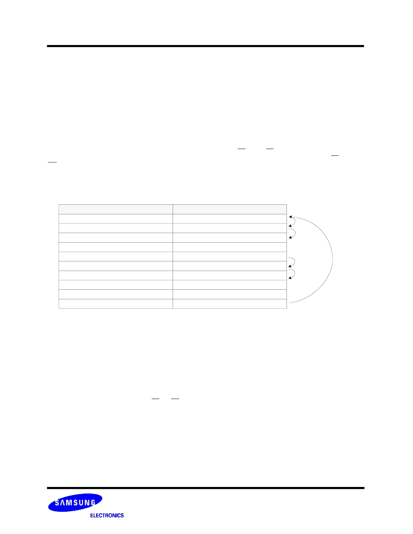
Synchronous Read Boundary
Division
Add.map(word order)
BootRAM Main(0.5Kw)
0000h~01FFh
BufferRAM0 Main(1Kw)
0200h~05FFh
BufferRAM1 Main(1Kw)
0600h~09FFh
Reserved Main
0A00h~7FFFh
BootRAM Spare(16w)
8000h~800Fh
BufferRAM0 Spare(32w)
8010h~802Fh
BufferRAM1 Spare(32w)
8030h~804Fh
Reserved Spare
8050h~8FFFh
Reserved Register
9000h~EFFFh
Register(4Kw)
F000h~FFFFh
Not Support
Not Support
* Reserved area is not available on Synchronous read
3.7.2.2 4-, 8-, 16-, 32-Word Linear Burst Read Operation
See Timing Diagram 6.1
An alternate Burst Read Mode enables a fixed number of words to be read from consecutive address.
The device supports a burst read from consecutive addresses of 4-, 8-, 16-, and 32-words with a linear-wrap around. When the last
word in the burst has been reached, assert CE and OE high to terminate the operation.
In this mode, the start address for the burst read can be any address of the address map with one exception. The device does not
support a 32-word linear burst read on the spare area of the BufferRAM.
Not Support
Not Support
Not Support
3.7.2.1 Continuous Linear Burst Read Operation
See Timing Diagram 6.2
相關(guān)PDF資料 |
PDF描述 |
|---|---|
| KFW1G16D2M-DID6 | FLASH MEMORY(54MHz) |
| KFW1G16Q2M-DEB5 | FLASH MEMORY(54MHz) |
| KFG1G16U2M-DEB | FLASH MEMORY |
| KFH1G16U2M-DEB | FLASH MEMORY |
| KFG1G16Q2M-DEB6 | FLASH MEMORY(66MHz) |
相關(guān)代理商/技術(shù)參數(shù) |
參數(shù)描述 |
|---|---|
| KFW1G16D2M-DID6 | 制造商:SAMSUNG 制造商全稱:Samsung semiconductor 功能描述:FLASH MEMORY(54MHz) |
| KFW1G16Q2M-DEB5 | 制造商:SAMSUNG 制造商全稱:Samsung semiconductor 功能描述:FLASH MEMORY(54MHz) |
| KFW1G16Q2M-DEB6 | 制造商:SAMSUNG 制造商全稱:Samsung semiconductor 功能描述:FLASH MEMORY(66MHz) |
| KFW1G16Q2M-DED5 | 制造商:SAMSUNG 制造商全稱:Samsung semiconductor 功能描述:FLASH MEMORY(54MHz) |
| KFW1G16Q2M-DED6 | 制造商:SAMSUNG 制造商全稱:Samsung semiconductor 功能描述:FLASH MEMORY(66MHz) |
發(fā)布緊急采購(gòu),3分鐘左右您將得到回復(fù)。