- 您現(xiàn)在的位置:買賣IC網(wǎng) > PDF目錄377611 > LC5512MC-45F256C (LATTICE SEMICONDUCTOR CORP) 3.3V, 2.5V and 1.8V In-System Programmable eXpanded Programmable Logic Device XPLD⑩ Family PDF資料下載
參數(shù)資料
| 型號(hào): | LC5512MC-45F256C |
| 廠商: | LATTICE SEMICONDUCTOR CORP |
| 元件分類: | PLD |
| 英文描述: | 3.3V, 2.5V and 1.8V In-System Programmable eXpanded Programmable Logic Device XPLD⑩ Family |
| 中文描述: | EE PLD, 5.7 ns, PBGA256 |
| 封裝: | FPBGA-256 |
| 文件頁(yè)數(shù): | 34/92頁(yè) |
| 文件大小: | 378K |
| 代理商: | LC5512MC-45F256C |
第1頁(yè)第2頁(yè)第3頁(yè)第4頁(yè)第5頁(yè)第6頁(yè)第7頁(yè)第8頁(yè)第9頁(yè)第10頁(yè)第11頁(yè)第12頁(yè)第13頁(yè)第14頁(yè)第15頁(yè)第16頁(yè)第17頁(yè)第18頁(yè)第19頁(yè)第20頁(yè)第21頁(yè)第22頁(yè)第23頁(yè)第24頁(yè)第25頁(yè)第26頁(yè)第27頁(yè)第28頁(yè)第29頁(yè)第30頁(yè)第31頁(yè)第32頁(yè)第33頁(yè)當(dāng)前第34頁(yè)第35頁(yè)第36頁(yè)第37頁(yè)第38頁(yè)第39頁(yè)第40頁(yè)第41頁(yè)第42頁(yè)第43頁(yè)第44頁(yè)第45頁(yè)第46頁(yè)第47頁(yè)第48頁(yè)第49頁(yè)第50頁(yè)第51頁(yè)第52頁(yè)第53頁(yè)第54頁(yè)第55頁(yè)第56頁(yè)第57頁(yè)第58頁(yè)第59頁(yè)第60頁(yè)第61頁(yè)第62頁(yè)第63頁(yè)第64頁(yè)第65頁(yè)第66頁(yè)第67頁(yè)第68頁(yè)第69頁(yè)第70頁(yè)第71頁(yè)第72頁(yè)第73頁(yè)第74頁(yè)第75頁(yè)第76頁(yè)第77頁(yè)第78頁(yè)第79頁(yè)第80頁(yè)第81頁(yè)第82頁(yè)第83頁(yè)第84頁(yè)第85頁(yè)第86頁(yè)第87頁(yè)第88頁(yè)第89頁(yè)第90頁(yè)第91頁(yè)第92頁(yè)
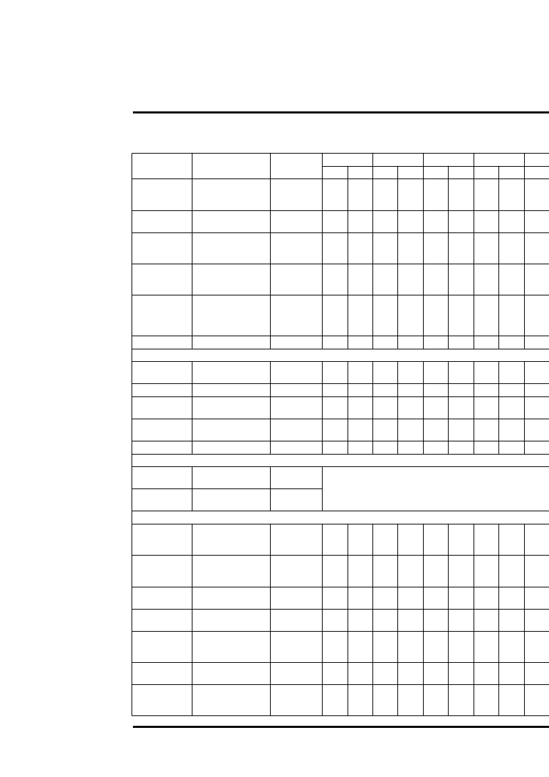
Lattice Semiconductor
ispXPLD 5000MX Family Data Sheet
34
t
CASC
Additional Delay for
PT Cascading
between MFBs
Carry Chain Delay,
MFB to MFB
Carry Chain Delay,
Macro-Cell to
Macro-Cell
Routing Delay for
Extended Function
Flags
Additional Flag
Delay when
Expanding Data
Widths
Counter Sum Delay
—
—
0.71
—
0.80
—
0.89
—
0.92
—
1.33
ns
t
CICOMFB
—
—
0.35
—
0.39
—
0.44
—
0.46
—
0.66
ns
t
CICOMC
—
—
0.10
—
0.11
—
0.13
—
0.13
—
0.19
ns
t
FLAG
—
—
2.62
—
2.94
—
3.27
—
3.40
—
4.91
ns
t
FLAGEXP
t
FLAGFULL
,
t
FLAGAFULL,
t
FLAGEMPTY
,
t
FLAGAEMPTY
t
PTSA
—
2.57
—
2.89
—
3.21
—
3.34
—
4.82
ns
t
SUM
Optional Adjusters
—
0.80
—
0.90
—
1.00
—
1.04
—
1.50
ns
t
BLA
Block Loading
Adder
PT Expander Adder
Additional Delay for
the Input Register
Secondary PLL
Output Delay
MFB Input Extender
t
ROUTE
—
0.04
—
0.04
—
0.05
—
0.05
—
0.07
ns
t
EXP
t
ROUTE
—
0.53
—
0.60
—
0.66
—
0.69
—
0.99
ns
t
INDIO
t
INREG
—
0.50
—
0.56
—
0.63
—
0.65
—
0.94
ns
t
PLL_SEC_DELAY
t
PLL_DELAY
—
0.91
—
0.91
—
0.91
—
0.91
—
0.91
ns
t
INEXP
Input and Output Buffer Delays
Input Buffer Selec-
tion Adder
Output Buffer
Selection Adder
FIFO
Write Data Setup
before Write Clock
Time
Write Data Hold
after Write Clock
Time
Opposite Clock
Cycle Delay
Write Clock to Full
Flag Delay
Write Clock to
Almost Full Flag
Delay
Read Clock to
Empty Flag Delay
Read Clock to
Almost Empty Flag
Delay
t
ROUTE
—
0.62
—
0.70
—
0.78
—
0.81
—
1.16
ns
t
IOI
t
GCLK_IN,
t
IN,
t
GOE,
t
RST
Refer to sysIO Adjuster Tables
ns
t
IOO
t
BUF
t
FIFOWCLKS
—
-0.27
—
-0.27
—
-0.22
—
-0.22
—
-0.21
—
ns
t
FIFOWCLKH
—
-0.01
—
-0.01
—
-0.01
—
-0.01
—
-0.01
—
ns
t
FIFOCLKSKEW
—
—
1.40
—
1.40
—
1.76
—
1.76
—
1.83
ns
t
FIFOFULL
—
—
3.08
—
3.08
—
3.85
—
3.85
—
4.00
ns
t
FIFOAFULL
—
—
3.08
—
3.08
—
3.86
—
3.86
—
4.01
ns
t
FIFOEMPTY
—
—
3.08
—
3.08
—
3.86
—
3.86
—
4.01
ns
t
FIFOAEMPTY
—
—
3.08
—
3.08
—
3.86
—
3.86
—
4.01
ns
ispXPLD 5000MX Family Internal Switching Characteristics (Continued)
Over Recommended Operating Conditions
Parameter
Description
Base
Parameter
-4
-45
-5
-52
-75
Units
Min.
Max.
Min.
Max.
Min.
Max.
Min.
Max.
Min.
Max.
相關(guān)PDF資料 |
PDF描述 |
|---|---|
| LC5512MC-45F484C | 3.3V, 2.5V and 1.8V In-System Programmable eXpanded Programmable Logic Device XPLD⑩ Family |
| LC5512MC-45Q208C | 3.3V, 2.5V and 1.8V In-System Programmable eXpanded Programmable Logic Device XPLD⑩ Family |
| LC5512MC-75F256C | 3.3V, 2.5V and 1.8V In-System Programmable eXpanded Programmable Logic Device XPLD⑩ Family |
| LC5512MC-75F484C | 3.3V, 2.5V and 1.8V In-System Programmable eXpanded Programmable Logic Device XPLD⑩ Family |
| LC5512MC-75Q208C | 3.3V, 2.5V and 1.8V In-System Programmable eXpanded Programmable Logic Device XPLD⑩ Family |
相關(guān)代理商/技術(shù)參數(shù) |
參數(shù)描述 |
|---|---|
| LC5512MC-45F256I | 制造商:LATTICE 制造商全稱:Lattice Semiconductor 功能描述:3.3V, 2.5V and 1.8V In-System Programmable eXpanded Programmable Logic Device XPLD⑩ Family |
| LC5512MC-45F484C | 功能描述:CPLD - 復(fù)雜可編程邏輯器件 PROGRAM EXPANDED LOG RoHS:否 制造商:Lattice 系列: 存儲(chǔ)類型:EEPROM 大電池?cái)?shù)量:128 最大工作頻率:333 MHz 延遲時(shí)間:2.7 ns 可編程輸入/輸出端數(shù)量:64 工作電源電壓:3.3 V 最大工作溫度:+ 90 C 最小工作溫度:0 C 封裝 / 箱體:TQFP-100 |
| LC5512MC-45F484I | 制造商:LATTICE 制造商全稱:Lattice Semiconductor 功能描述:3.3V, 2.5V and 1.8V In-System Programmable eXpanded Programmable Logic Device XPLD⑩ Family |
| LC5512MC-45F672C | 制造商:LATTICE 制造商全稱:Lattice Semiconductor 功能描述:3.3V, 2.5V and 1.8V In-System Programmable eXpanded Programmable Logic Device XPLD⑩ Family |
| LC5512MC-45F672I | 制造商:LATTICE 制造商全稱:Lattice Semiconductor 功能描述:3.3V, 2.5V and 1.8V In-System Programmable eXpanded Programmable Logic Device XPLD⑩ Family |
發(fā)布緊急采購(gòu),3分鐘左右您將得到回復(fù)。