- 您現(xiàn)在的位置:買賣IC網(wǎng) > PDF目錄377798 > LXT332 (Digital Data Communications GmbH) 3941 PDF資料下載
參數(shù)資料
| 型號(hào): | LXT332 |
| 廠商: | Digital Data Communications GmbH |
| 英文描述: | 3941 |
| 中文描述: | 雙T1/E1線路接口單元與水晶無(wú)衰減 |
| 文件頁(yè)數(shù): | 7/32頁(yè) |
| 文件大小: | 777K |
| 代理商: | LXT332 |
第1頁(yè)第2頁(yè)第3頁(yè)第4頁(yè)第5頁(yè)第6頁(yè)當(dāng)前第7頁(yè)第8頁(yè)第9頁(yè)第10頁(yè)第11頁(yè)第12頁(yè)第13頁(yè)第14頁(yè)第15頁(yè)第16頁(yè)第17頁(yè)第18頁(yè)第19頁(yè)第20頁(yè)第21頁(yè)第22頁(yè)第23頁(yè)第24頁(yè)第25頁(yè)第26頁(yè)第27頁(yè)第28頁(yè)第29頁(yè)第30頁(yè)第31頁(yè)第32頁(yè)
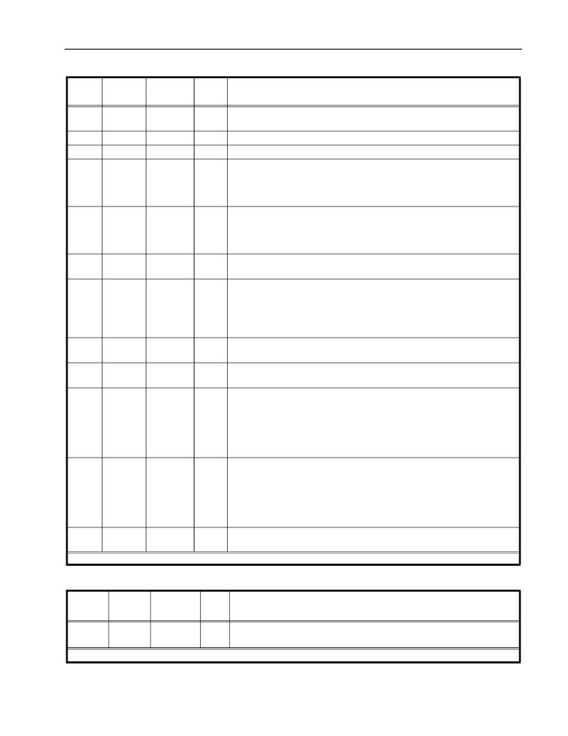
L1
eììê
/;7êê 'XDO 7ì(ì /LQH ,QWHUIDFH 8QLW ZLWK &U\VWDOeOHVV -LWWHU $WWHQXDWLRQ
é
êí
TVCC1
AI
+ 5 volt power supply input for the port 1 transmit driver.
TVCC1 must
not vary from TVCC0 or VCC by more than ± 0.3 V.
Ground.
Ground return for power supply TVCC1.
+5 VDC power supply
input for all circuits, except the transmit drivers.
Jitter Attenuation Select.
Selects jitter attenuation for both ports. When
JASEL = 1, JA circuits are placed in the receive paths. When JASEL = 0, JA
circuits are placed in the transmit paths. When JASEL is clocked with
MCLK, the JA circuit is disabled.
Violation insert, Clock, or QRSS.
Function (Violation insert, Clock, or
QRSS) is determined by the VCQE pin. Provides Violation Insertion, High
Frequency Clock or QRSS Generation functions for Port 1. Refer to VCQ0
signal description for details.
Serial Port Enable.
SPE must be clocked with MCLK to enable Host Mode
control through the serial port.
Violation - Clock - QRSS Enable.
When set High, enables the Bipolar
Violation Insert functions of VCQ0 and VCQ1 pins. When set Low, enables
the High Frequency Clock functions of VCQ0 and VCQ1. When clocked
with MCLK, enables the QRSS functions of VCQ0 and VCQ1, and enables
the QRSS Generate and Detect function of PD0 and PD1 pins.
Serial Data Output.
If CLKE is High, SDO is valid on the rising edge of
SCLK. If CLKE is Low, SDO is valid on the falling edge of SCLK.
Receive Clock - Port 1.
This clock is recovered from the input signal.
Under Loss of Signal (LOS) conditions, this output is derived from MCLK.
Receive Positive and Negative Data - Port 1.
In the Bipolar I/O mode,
these pins are the data outputs from port 1. A signal on RPOS corresponds to
receipt of a positive pulse on RTIP/RRING. A signal on RNEG corresponds
to receipt of a negative pulse on RTIP/RRING. RNEG/RPOS outputs are
Non-Return-to-Zero (NRZ). CLKE determines the clock edge at which
these outputs are stable and valid.
Transmit Positive and Negative Data - Port 1.
In the Bipolar I/O mode,
these pins are TPOS and TNEG, the positive and negative sides of a bipolar
input pair for port 1. Data to be transmitted onto the twisted-pair line is input
at these pins. However, when TRSTE is clocked by MCLK, the LXT332
switches to a unipolar mode. Unipolar mode pin functions are described sep-
arately.
Transmit Clock - Port 1.
1.544 MHz for T1, 2.048 MHz for E1. The trans-
mit data inputs are sampled on the falling edge of TCLK.
è
êì
êê
êé
TGND1
VCC
JASEL
–
AI
DI
êè
VCQ1
DI/O
êí
ê
SPE
DI
êì
ê
VCQE
DI
ê
ê
SDO
DO
êê
ê
RCLK1
DO
êé
êè
éí
éì
RPOS1
(Bipolar)
RNEG1
(Bipolar)
DO
DO
ê
ê
é
éê
TNEG1
(Bipolar)
TPOS1
(Bipolar)
DI
DI
ê
éé
TCLK1
DI
7DEOH 8QLSRODU +RVW 0RGH 3LQ 'HVFULSWLRQV
ì
3LQ
4)3
3LQ
3/&&
6\PERO
,2
'HVFULSWLRQ
éì
ê
TDATA0
DI
Transmit Data - Port 0.
In the Unipolar mode, the data to be transmitted
onto the twisted-pair line from port 0 is input at this pin.
ì 7DEOH ì GHVFULEHV WKH SLQV WKDW GR QRW FKDQJH IXQFWLRQ LQ 8QLSRODU +RVW 0RGH DQG IXQFWLRQV RI SLQV XQLTXH WR %LSRODU 0RGH
7DEOH ì +RVW 0RGH 3LQ DQG %LSRODU +RVW 0RGH 3LQ 'HVFULSWLRQV
¤ FRQWLQXHG
3LQ
4)3
3LQ
3/&&
6\PERO
,2
ì
'HVFULSWLRQ
ì ', 'LJLWDO ,QSXWa '2 'LJLWDO 2XWSXWa ',2 'LJLWDO ,QSXW2XWSXWa $, $QDORJ ,QSXWa $2 $QDORJ 2XWSXW
相關(guān)PDF資料 |
PDF描述 |
|---|---|
| LXT334 | Quad Short Haul Transceiver with Clock Recovery |
| LXT335 | Quad Short Haul PCM Analog Interface |
| LXT350 | Integrated T1/E1 S/H Transceivers With Crystal-less Jitter Attenuation |
| LXT350QE | Integrated T1/E1 S/H Transceivers With Crystal-less Jitter Attenuation |
| LXT351 | T1/E1 Short Haul Transceiver with Crystal-less Jitter Attenuation |
相關(guān)代理商/技術(shù)參數(shù) |
參數(shù)描述 |
|---|---|
| LXT332PE | 制造商:未知廠家 制造商全稱:未知廠家 功能描述:Line Interface |
| LXT332QE | 制造商:未知廠家 制造商全稱:未知廠家 功能描述:Line Interface |
| LXT334 | 制造商:LVL1 制造商全稱:LVL1 功能描述:Quad Short Haul Transceiver with Clock Recovery |
| LXT334&LXT304A | 制造商:未知廠家 制造商全稱:未知廠家 功能描述:LXT334 & LXT304A - LXT334 & LXT304A ?Low Cost & High Performance Quad E1 Interface Solution |
| LXT335 | 制造商:LVL1 制造商全稱:LVL1 功能描述:Quad Short Haul PCM Analog Interface |
發(fā)布緊急采購(gòu),3分鐘左右您將得到回復(fù)。