- 您現(xiàn)在的位置:買賣IC網(wǎng) > PDF目錄180205 > M393B1K73CH0-YH9 1G X 72 MULTI DEVICE DRAM MODULE, 0.255 ns, DMA240 PDF資料下載
參數(shù)資料
| 型號(hào): | M393B1K73CH0-YH9 |
| 元件分類: | DRAM |
| 英文描述: | 1G X 72 MULTI DEVICE DRAM MODULE, 0.255 ns, DMA240 |
| 封裝: | HALOGEN FREE AND ROHS COMPLIANT, DIMM-240 |
| 文件頁(yè)數(shù): | 17/53頁(yè) |
| 文件大小: | 1492K |
| 代理商: | M393B1K73CH0-YH9 |
第1頁(yè)第2頁(yè)第3頁(yè)第4頁(yè)第5頁(yè)第6頁(yè)第7頁(yè)第8頁(yè)第9頁(yè)第10頁(yè)第11頁(yè)第12頁(yè)第13頁(yè)第14頁(yè)第15頁(yè)第16頁(yè)當(dāng)前第17頁(yè)第18頁(yè)第19頁(yè)第20頁(yè)第21頁(yè)第22頁(yè)第23頁(yè)第24頁(yè)第25頁(yè)第26頁(yè)第27頁(yè)第28頁(yè)第29頁(yè)第30頁(yè)第31頁(yè)第32頁(yè)第33頁(yè)第34頁(yè)第35頁(yè)第36頁(yè)第37頁(yè)第38頁(yè)第39頁(yè)第40頁(yè)第41頁(yè)第42頁(yè)第43頁(yè)第44頁(yè)第45頁(yè)第46頁(yè)第47頁(yè)第48頁(yè)第49頁(yè)第50頁(yè)第51頁(yè)第52頁(yè)第53頁(yè)
- 17 -
datasheet
DDR3L SDRAM
Rev. 1.01
Registered DIMM
NOTE :
1. For input only pins except RESET, VREF = VREFDQ(DC)
2. See "Overshoot and Undershoot specifications" section.
3. The AC peak noise on VREF may not allow VREF to deviate from VREF(DC) by more than ± 1% VDD (for reference : approx. ± 15mV)
4. For reference : approx. VDD/2 ± 15mV
5. Single ended swing requirement for DQS - DQS is 350mV (peak to peak). Differential swing requirement for DQS - DQS is 700mV (peak to peak).
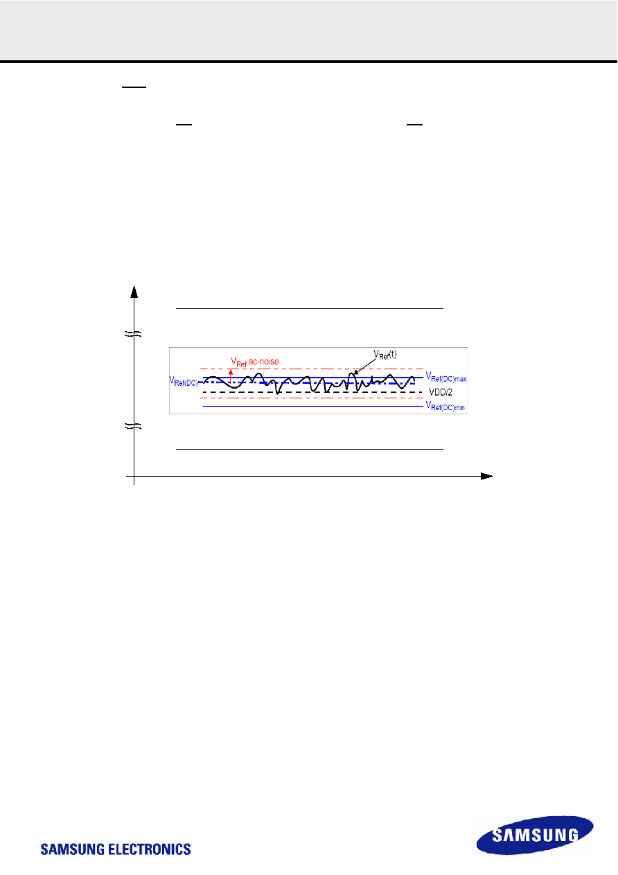
13.2 VREF Tolerances
The dc-tolerance limits and ac-noise limits for the reference voltages VREFCA and VREFDQ are illustrate in Figure 1. It shows a valid reference voltage
VREF(t) as a function of time. (VREF stands for VREFCA and VREFDQ likewise).
VREF(DC) is the linear average of VREF(t) over a very long period of time (e.g. 1 sec). This average has to meet the min/max requirements of VREF. Fur-
thermore VREF(t) may temporarily deviate from VREF(DC) by no more than ± 1% VDD.
Figure 1. Illustration of VREF(DC) tolerance and VREF ac-noise limits
The voltage levels for setup and hold time measurements VIH(AC), VIH(DC), VIL(AC) and VIL(DC) are dependent on VREF.
This clarifies, that dc-variations of VREF affect the absolute voltage a signal has to reach to achieve a valid high or low level and therefore the time to
which setup and hold is measured. System timing and voltage budgets need to account for VREF(DC) deviations from the optimum position within the
data-eye of the input signals.
This also clarifies that the DRAM setup/hold specification and derating values need to include time and voltage associated with VREF ac-noise.
Timing and voltage effects due to ac-noise on VREF up to the specified limit (+/-1% of VDD) are included in DRAM timings and their associated deratings.
voltage
VDD
VSS
time
相關(guān)PDF資料 |
PDF描述 |
|---|---|
| M393B5273CH0-CK0 | 512M X 72 MULTI DEVICE DRAM MODULE, 0.225 ns, DMA240 |
| M393B5773CH0-CK0 | 256M X 72 MULTI DEVICE DRAM MODULE, 0.225 ns, DMA240 |
| M3950/1529A012 | TOGGLE SWITCH, 3PDT, LATCHED, 4A, 28VDC, THROUGH HOLE-STRAIGHT |
| M83731/2327D110 | TOGGLE SWITCH, 3PDT, MOMENTARY, 4A, 28VDC, THROUGH HOLE-STRAIGHT |
| M3950/1726A110 | TOGGLE SWITCH, 3PDT, LATCHED, 4A, 28VDC, THROUGH HOLE-STRAIGHT |
相關(guān)代理商/技術(shù)參數(shù) |
參數(shù)描述 |
|---|---|
| M393B1K73EB0 | 制造商:SAMSUNG 制造商全稱:Samsung semiconductor 功能描述:240pin Registered DIMM based on 2Gb E-die |
| M393B273DH0-CH9E8 | 制造商:Samsung Semiconductor 功能描述:4GB 2RX8 PC3-8500R-07-00-B0-D1 - Trays |
| M393B2873EH1 | 制造商:SAMSUNG 制造商全稱:Samsung semiconductor 功能描述:DDR3 SDRAM Memory |
| M393B2873EH1-CF8 | 制造商:ATP Electronics Inc 功能描述:M393B2873EH1-CF8 - Bulk |
| M393B2873FH0 | 制造商:SAMSUNG 制造商全稱:Samsung semiconductor 功能描述:DDR3 SDRAM Memory |
發(fā)布緊急采購(gòu),3分鐘左右您將得到回復(fù)。
