- 您現(xiàn)在的位置:買賣IC網(wǎng) > PDF目錄180205 > M393B1K73CH0-YH9 1G X 72 MULTI DEVICE DRAM MODULE, 0.255 ns, DMA240 PDF資料下載
參數(shù)資料
| 型號: | M393B1K73CH0-YH9 |
| 元件分類: | DRAM |
| 英文描述: | 1G X 72 MULTI DEVICE DRAM MODULE, 0.255 ns, DMA240 |
| 封裝: | HALOGEN FREE AND ROHS COMPLIANT, DIMM-240 |
| 文件頁數(shù): | 21/53頁 |
| 文件大?。?/td> | 1492K |
| 代理商: | M393B1K73CH0-YH9 |
第1頁第2頁第3頁第4頁第5頁第6頁第7頁第8頁第9頁第10頁第11頁第12頁第13頁第14頁第15頁第16頁第17頁第18頁第19頁第20頁當(dāng)前第21頁第22頁第23頁第24頁第25頁第26頁第27頁第28頁第29頁第30頁第31頁第32頁第33頁第34頁第35頁第36頁第37頁第38頁第39頁第40頁第41頁第42頁第43頁第44頁第45頁第46頁第47頁第48頁第49頁第50頁第51頁第52頁第53頁
- 21 -
datasheet
DDR3L SDRAM
Rev. 1.01
Registered DIMM
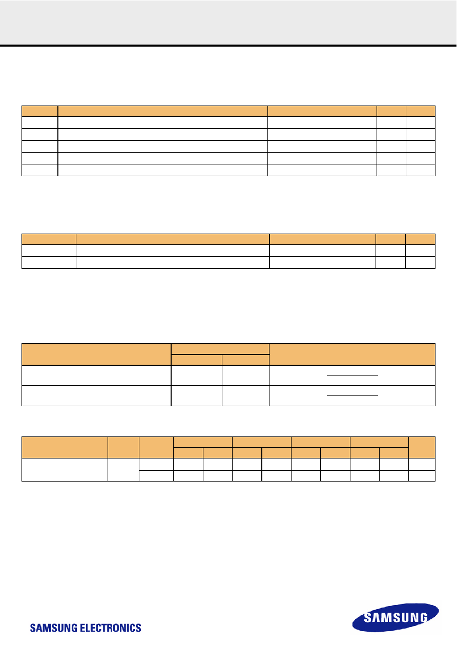
14. AC & DC Output Measurement Levels
14.1 Single Ended AC and DC Output Levels
[ Table 8 ] Single Ended AC and DC output levels
NOTE : 1. The swing of +/-0.1 x VDDQ is based on approximately 50% of the static single ended output high or low swing with a driver impedance of 40Ω and an effective test
load of 25
Ω to VTT=VDDQ/2.
14.2 Differential AC and DC Output Levels
[ Table 9 ] Differential AC and DC output levels
NOTE : 1. The swing of +/-0.2xVDDQ is based on approximately 50% of the static single ended output high or low swing with a driver impedance of 40Ω and an effective test
load of 25
Ω to VTT=VDDQ/2 at each of the differential outputs.
14.3 Single-ended Output Slew Rate
With the reference load for timing measurements, output slew rate for falling and rising edges is defined and measured between VOL(AC) and VOH(AC)
for single ended signals as shown in below.
[ Table 10 ] Single ended Output slew rate definition
NOTE : Output slew rate is verified by design and characterization, and may not be subject to production test.
[ Table 11 ] Single ended output slew rate
Description : SR : Slew Rate
Q : Query Output (like in DQ, which stands for Data-in, Query-Output)
se : Single-ended Signals, For Ron = RZQ/7 setting
NOTE : 1) In two cased, a maximum slew rate of 6V/ns applies for a single DQ signal within a byte lane.
- Case_1 is defined for a single DQ signal within a byte lane which is switching into a certain direction (either from high to low of low to high) while all remaining DQ
signals in the same byte lane are static (i.e they stay at either high or low).
- Case_2 is defined for a single DQ signals in the same byte lane are switching into the opposite direction (i.e. from low to high or high to low respectively). For the
remaining DQ signal switching into the opposite direction, the regular maximum limit of 5 V/ns applies.
Symbol
Parameter
DDR3-800/1066/1333/1600
Units
NOTE
VOH(DC) DC output high measurement level (for IV curve linearity)
0.8 x VDDQ
V
VOM(DC) DC output mid measurement level (for IV curve linearity)
0.5 x VDDQ
V
VOL(DC) DC output low measurement level (for IV curve linearity)
0.2 x VDDQ
V
VOH(AC) AC output high measurement level (for output SR)
VTT + 0.1 x VDDQ
V1
VOL(AC) AC output low measurement level (for output SR)
VTT - 0.1 x VDDQ
V1
Symbol
Parameter
DDR3-800/1066/1333/1600
Units
NOTE
VOHdiff(AC)
AC differential output high measurement level (for output SR)
+0.2 x VDDQ
V1
VOLdiff(AC)
AC differential output low measurement level (for output SR)
-0.2 x VDDQ
V1
Description
Measured
Defined by
From
To
Single ended output slew rate for rising edge
VOL(AC)
VOH(AC)
VOH(AC)-VOL(AC)
Delta TRse
Single ended output slew rate for falling edge
VOH(AC)
VOL(AC)
VOH(AC)-VOL(AC)
Delta TFse
Parameter
Symbol
Operation
Voltage
DDR3-800
DDR3-1066
DDR3-1333
DDR3-1600
Units
Min
Max
Min
Max
Min
Max
Min
Max
Single ended output slew rate
SRQse
1.35V
1.75
51)
1.75
51)
-
TBD
V/ns
1.5V
2.5
5
2.5
5
2.5
5
TBD
5
V/ns
相關(guān)PDF資料 |
PDF描述 |
|---|---|
| M393B5273CH0-CK0 | 512M X 72 MULTI DEVICE DRAM MODULE, 0.225 ns, DMA240 |
| M393B5773CH0-CK0 | 256M X 72 MULTI DEVICE DRAM MODULE, 0.225 ns, DMA240 |
| M3950/1529A012 | TOGGLE SWITCH, 3PDT, LATCHED, 4A, 28VDC, THROUGH HOLE-STRAIGHT |
| M83731/2327D110 | TOGGLE SWITCH, 3PDT, MOMENTARY, 4A, 28VDC, THROUGH HOLE-STRAIGHT |
| M3950/1726A110 | TOGGLE SWITCH, 3PDT, LATCHED, 4A, 28VDC, THROUGH HOLE-STRAIGHT |
相關(guān)代理商/技術(shù)參數(shù) |
參數(shù)描述 |
|---|---|
| M393B1K73EB0 | 制造商:SAMSUNG 制造商全稱:Samsung semiconductor 功能描述:240pin Registered DIMM based on 2Gb E-die |
| M393B273DH0-CH9E8 | 制造商:Samsung Semiconductor 功能描述:4GB 2RX8 PC3-8500R-07-00-B0-D1 - Trays |
| M393B2873EH1 | 制造商:SAMSUNG 制造商全稱:Samsung semiconductor 功能描述:DDR3 SDRAM Memory |
| M393B2873EH1-CF8 | 制造商:ATP Electronics Inc 功能描述:M393B2873EH1-CF8 - Bulk |
| M393B2873FH0 | 制造商:SAMSUNG 制造商全稱:Samsung semiconductor 功能描述:DDR3 SDRAM Memory |
發(fā)布緊急采購,3分鐘左右您將得到回復(fù)。