- 您現(xiàn)在的位置:買賣IC網 > PDF目錄377830 > M52S128168A (Elite Semiconductor Memory Technology Inc.) 1M x 16 Bit x 4 Banks Synchronous DRAM PDF資料下載
參數資料
| 型號: | M52S128168A |
| 廠商: | Elite Semiconductor Memory Technology Inc. |
| 英文描述: | 1M x 16 Bit x 4 Banks Synchronous DRAM |
| 中文描述: | 100萬× 16位× 4個銀行同步DRAM |
| 文件頁數: | 3/47頁 |
| 文件大小: | 1213K |
| 代理商: | M52S128168A |
第1頁第2頁當前第3頁第4頁第5頁第6頁第7頁第8頁第9頁第10頁第11頁第12頁第13頁第14頁第15頁第16頁第17頁第18頁第19頁第20頁第21頁第22頁第23頁第24頁第25頁第26頁第27頁第28頁第29頁第30頁第31頁第32頁第33頁第34頁第35頁第36頁第37頁第38頁第39頁第40頁第41頁第42頁第43頁第44頁第45頁第46頁第47頁
ES MT
Preliminary
M52S128168A
Elite Semiconductor Memory Technology Inc.
Revision
:
1.0
Publication Date
:
May. 2007
3/47
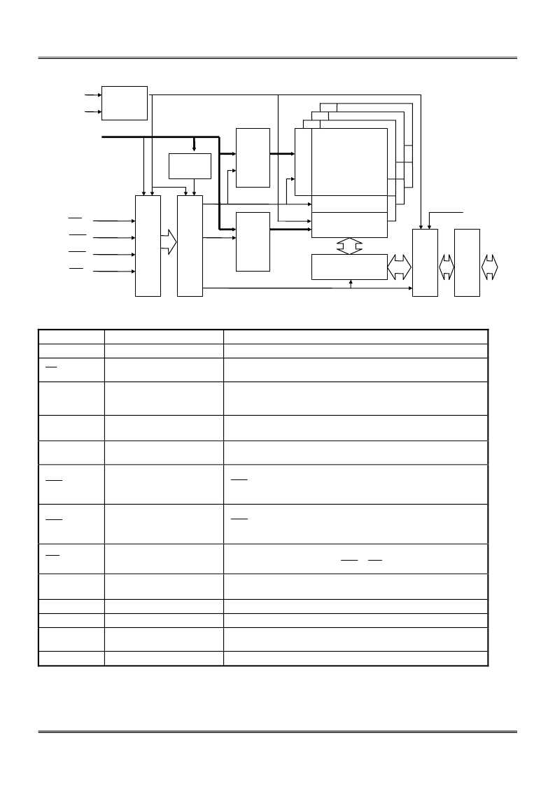
FUNCTIONAL BLOCK DIAGRAM
PIN FUNCTION DESCRIPTION
PIN
NAME
INPUT FUNCTION
CLK
System Clock
Active on the positive going edge to sample all inputs
Disables or enables device operation by masking or enabling all
inputs except CLK , CKE and L(U)DQM
CS
Chip Select
CKE
Clock Enable
Masks system clock to freeze operation from the next clock cycle.
CKE should be enabled at least one cycle prior new command.
Disable input buffers for power down in standby.
A0 ~ A11
Address
Row / column address are multiplexed on the same pins.
Row address : RA0~RA11, column address : CA0~CA7
BA0 , BA1
Bank Select Address
Selects bank to be activated during row address latch time.
Selects bank for read / write during column address latch time.
RAS
Row Address Strobe
Latches row addresses on the positive going edge of the CLK with
RAS low.
Enables row access & precharge.
CAS
Column Address Strobe
Latches column address on the positive going edge of the CLK with
CAS low.
Enables column access.
WE
Write Enable
Enables write operation and row precharge.
Latches data in starting from CAS ,
WE
active.
L(U)DQM
Data Input / Output Mask
Makes data output Hi-Z, t
SHZ
after the clock and masks the output.
Blocks data input when L(U)DQM active.
DQ0 ~ DQ15
Data Input / Output
Data inputs / outputs are multiplexed on the same pins.
VDD / VSS
Power Supply / Ground
Power and ground for the input buffers and the core logic.
Isolated power supply and ground for the output buffers to provide
improved noise immunity.
VDDQ / VSSQ Data Output Power / Ground
NC
No Connection
This pin is recommended to be left No Connection on the device.
L(U)DQM
DQ
Mode
Register
C
Column
Address
Buffer
&
Refresh
Counter
Row
Address
Buffer
&
Refresh
Counter
Bank D
Bank C
R
Bank A
Bank B
Sense Amplifier
Column Decoder
Data Control Circuit
L
I
B
Address
Clock
Generator
CLK
CKE
C
CS
RAS
CAS
WE
相關PDF資料 |
PDF描述 |
|---|---|
| M52S128168A-10BG | 1M x 16 Bit x 4 Banks Synchronous DRAM |
| M52S128168A-10TG | 1M x 16 Bit x 4 Banks Synchronous DRAM |
| M52S128168A-7.5BG | 1M x 16 Bit x 4 Banks Synchronous DRAM |
| M52S128168A-7.5TG | 1M x 16 Bit x 4 Banks Synchronous DRAM |
| M52S16161A | 512K x 16Bit x 2Banks Synchronous DRAM |
相關代理商/技術參數 |
參數描述 |
|---|---|
| M52S128168A_08 | 制造商:ESMT 制造商全稱:Elite Semiconductor Memory Technology Inc. 功能描述:2M x 16 Bit x 4 Banks Synchronous DRAM |
| M52S128168A-10BG | 制造商:ELITE SEMICONDUCTOR 功能描述:SDRAM 128MB 2.5V 100MHZ FBGA54 |
| M52S128168A-10TG | 制造商:ELITE SEMICONDUCTOR 功能描述:SDRAM 128MB 2.5V 100MHZ TSOPII54 |
| M52S128168A-7.5BG | 制造商:ELITE SEMICONDUCTOR 功能描述:SDRAM 128MB 2.5V 133MHZ FBGA54 制造商:ELITE SEMICONDUCTOR 功能描述:SDRAM, 128MB, 2.5V, 133MHZ, FBGA54 制造商:ELITE SEMICONDUCTOR 功能描述:DRAM IC; Page Size:128MB; Memory Case Style:FBGA; No. of Pins:54; IC Interface Type:Parallel; Operating Temperature Min:0C; Operating Temperature Max:70C; Filter Terminals:Surface Mount; Frequency:133MHz; Interface Type:Parallel ;RoHS Compliant: Yes |
| M52S128168A-7.5TG | 制造商:ELITE SEMICONDUCTOR 功能描述:SDRAM 128MB 2.5V 133MHZ TSOPII54 |
發(fā)布緊急采購,3分鐘左右您將得到回復。