- 您現(xiàn)在的位置:買(mǎi)賣(mài)IC網(wǎng) > PDF目錄383540 > MAX9222EUM (MAXIM INTEGRATED PRODUCTS INC) Programmable DC-Balance 21-Bit Deserializers PDF資料下載
參數(shù)資料
| 型號(hào): | MAX9222EUM |
| 廠商: | MAXIM INTEGRATED PRODUCTS INC |
| 元件分類(lèi): | 通用總線功能 |
| 英文描述: | Programmable DC-Balance 21-Bit Deserializers |
| 中文描述: | QUAD LINE RECEIVER, PDSO48 |
| 封裝: | 6.10 MM, MO-153ED, TSSOP-48 |
| 文件頁(yè)數(shù): | 14/18頁(yè) |
| 文件大小: | 904K |
| 代理商: | MAX9222EUM |
第1頁(yè)第2頁(yè)第3頁(yè)第4頁(yè)第5頁(yè)第6頁(yè)第7頁(yè)第8頁(yè)第9頁(yè)第10頁(yè)第11頁(yè)第12頁(yè)第13頁(yè)當(dāng)前第14頁(yè)第15頁(yè)第16頁(yè)第17頁(yè)第18頁(yè)
M
Programmable DC-Balance
21-Bit Deserializers
14
______________________________________________________________________________________
5V Tolerant Input
PWRDWN
is 5V tolerant and is internally pulled down to
GND. DCB/NC is not 5V tolerant. The input voltage
range for DCB/NC is nominally ground to V
CC
.
Normally, DCB/NC is connected to V
CC
or ground.
Skew Margin (RSKM)
Skew margin (RSKM) is the time allowed for degrada-
tion of the serial data sampling setup and hold times by
sources other than the deserializer. The deserializer
sampling uncertainty is accounted for and does not
need to be subtracted from RSKM. The main outside
contributors of jitter and skew that subtract from RSKM
are interconnect intersymbol interference, serializer
pulse position uncertainty, and pair-to-pair path skew.
V
CCO
Output Supply and Power Dissipation
The outputs have a separate supply (V
CCO
) for interfacing
to systems with 1.8V to 5V nominal input logic levels. The
DC Electrical Characteristics
table gives the maximum
supply current for V
CCO
= 3.6V with 8pF load at several
switching frequencies with all outputs switching in the
worst-case switching pattern. The approximate incremen-
tal supply current for V
CCO
other than 3.6V
with the same
8pF
load and worst-case pattern can be calculated using:
I
I
= C
T
V
I
0.5f
C
x 21 (data outputs)
+ C
T
V
I
f
C
x 1 (clock output)
where:
I
I
= incremental supply current.
C
T
= total internal (C
INT
) and external (C
L
) load capaci-
tance.
V
I
= incremental supply voltage.
f
C
= output clock switching frequency.
The incremental current is added to (for V
CCO
>
3.6V)
or subtracted from (for V
CCO
<
3.6V) the
DC Electrical
Characteristics
table maximum supply current. The
internal output buffer capacitance is C
INT
= 6pF. The
worst-case pattern switching frequency of the data out-
puts is half the switching frequency of the output clock.
In the following example, the incremental supply current is
calculated for V
CCO
= 5.5V, f
C
= 34MHz, and C
L
= 8pF:
V
I
= 5.5V - 3.6V = 1.9V
C
T
= C
INT
+ C
L
= 6pF + 8pF = 14pF
where:
I
I
= C
T
V
I
0.5F
C
x 21 (data outputs) + C
T
V
I
f
C
x 1 (clock
output).
I
I
= (14pF x 1.9V x 0.5 x 34MHz x 21) + (14pF x 1.9V x
34MHz).
I
I
= 9.5mA + 0.9mA = 10.4mA.
The maximum supply current in DC-balanced mode for
V
CC
= V
CCO
= 3.6V at f
C
= 34MHz is 106mA (from the
DC Electrical Characteristics
table). Add 10.4mA to get
the total approximate maximum supply current at V
CCO
= 5.5V and V
CC
= 3.6V.
If the output supply voltage is less than V
CCO
= 3.6V,
the reduced supply current can be calculated using the
same formula and method.
At high switching frequency, high supply voltage, and
high capacitive loading, power dissipation can exceed
the package power dissipation rating. Do not exceed
the maximum package power dissipation rating. See
the
Absolute Maximum Ratings
for maximum package
power dissipation capacity and temperature derating.
Rising- or Falling-Edge Output Strobe
The MAX9210/MAX9212/MAX9214/MAX9216 have a
rising-edge output strobe, which latches the parallel
output data into the next chip on the rising edge of
RxCLK OUT. The MAX9220/MAX9222 have a falling-
edge output strobe, which latches the parallel output
data into the next chip on the falling edge of RxCLK
OUT. The deserializer output strobe polarity does not
need to match the serializer input strobe polarity. A
deserializer with rising or falling edge output strobe can
be driven by a serializer with a rising edge input strobe.
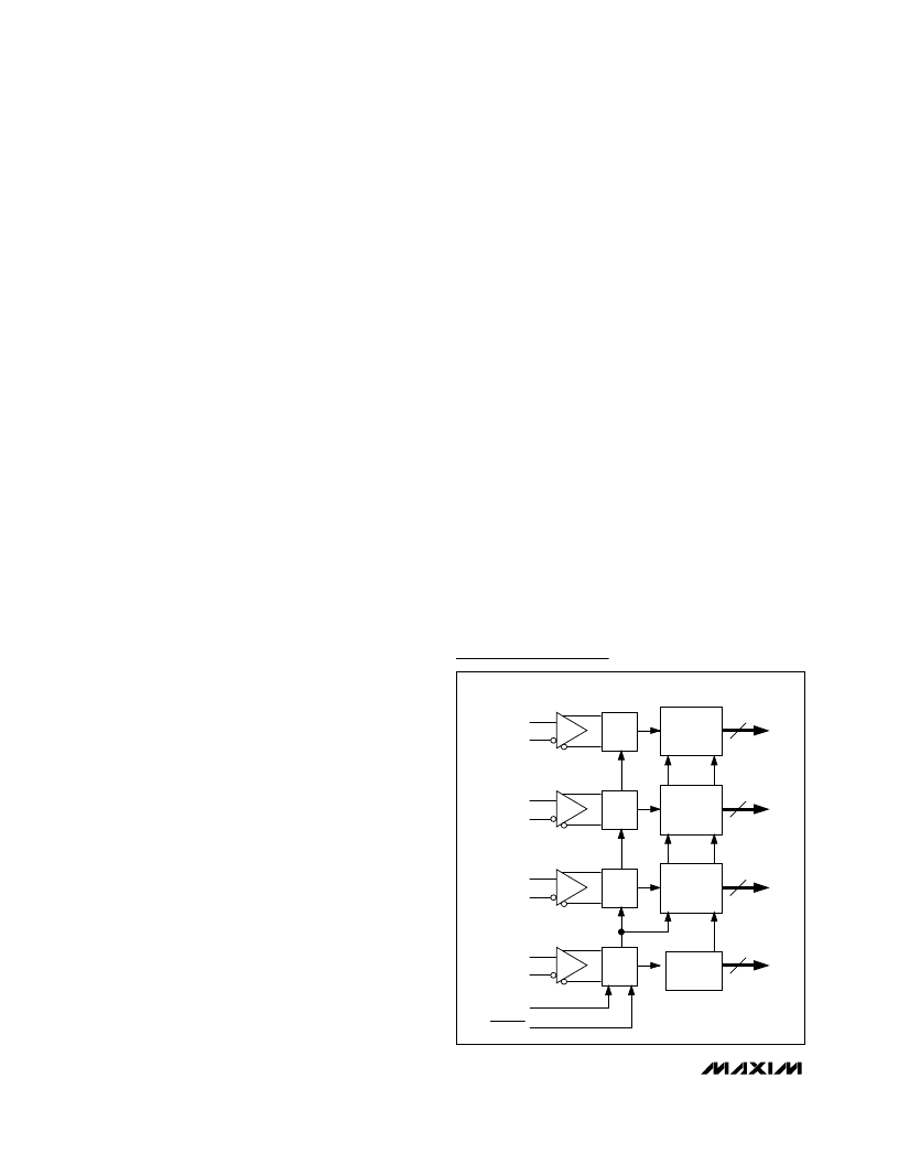
RxIN0+
LVDS DATA
RECEIVER 0
RxIN0-
STROBE
DATA
CHANNEL 0
RxOUT0–6
SERIAL-TO-
PARALLEL
CONVERTER
RxIN1+
LVDS DATA
RECEIVER 1
RxIN1-
STROBE
DATA
CHANNEL 1
RxOUT7–13
SERIAL-TO-
PARALLEL
CONVERTER
RxIN2+
LVDS DATA
RECEIVER 2
RxIN2-
STROBE
DATA
CHANNEL 2
RxOUT14–20
SERIAL-TO-
PARALLEL
CONVERTER
RxCLK IN+
LVDS CLOCK
RECEIVER
RxCLK IN-
DCB/NC
7x/9x
PLL
RxCLK OUT
REFERENCE
CLOCK
GENERATOR
PWRDWN
Functional Diagram
相關(guān)PDF資料 |
PDF描述 |
|---|---|
| MAX9212ETM | Programmable DC-Balance 21-Bit Deserializers |
| MAX9214ETM | Programmable DC-Balance 21-Bit Deserializers |
| MAX9220ETM | Programmable DC-Balance 21-Bit Deserializers |
| MAX9222ETM | Programmable DC-Balance 21-Bit Deserializers |
| MAX9216ETM | Programmable DC-Balance 21-Bit Deserializers |
相關(guān)代理商/技術(shù)參數(shù) |
參數(shù)描述 |
|---|---|
| MAX9222EUM+ | 制造商:Maxim Integrated Products 功能描述:LVDS DESERLIZER 48TSSOP - Rail/Tube |
| MAX9222EUM+D | 制造商:Maxim Integrated Products 功能描述:LVDS DESERLIZER 48TSSOP - Rail/Tube |
| MAX9222EUM+T | 制造商:Maxim Integrated Products 功能描述:LVDS DESERLIZER 48TSSOP - Tape and Reel |
| MAX9222EUM+TD | 制造商:Maxim Integrated Products 功能描述:- Tape and Reel |
| MAX9222EUM-D | 制造商:Maxim Integrated Products 功能描述:PROGRAMMABLE DC-BALANCE 21-BIT DESERIALIZERS - Rail/Tube |
發(fā)布緊急采購(gòu),3分鐘左右您將得到回復(fù)。