- 您現(xiàn)在的位置:買賣IC網(wǎng) > PDF目錄377882 > MB582A (Fujitsu Limited) 155-Mbps ATM Transceiver(155Mbps 異步傳輸模式 收發(fā)器) PDF資料下載
參數(shù)資料
| 型號: | MB582A |
| 廠商: | Fujitsu Limited |
| 英文描述: | 155-Mbps ATM Transceiver(155Mbps 異步傳輸模式 收發(fā)器) |
| 中文描述: | 155 - Mbps的自動柜員機收發(fā)器(155Mbps異步傳輸模式收發(fā)器) |
| 文件頁數(shù): | 5/46頁 |
| 文件大?。?/td> | 345K |
| 代理商: | MB582A |
第1頁第2頁第3頁第4頁當前第5頁第6頁第7頁第8頁第9頁第10頁第11頁第12頁第13頁第14頁第15頁第16頁第17頁第18頁第19頁第20頁第21頁第22頁第23頁第24頁第25頁第26頁第27頁第28頁第29頁第30頁第31頁第32頁第33頁第34頁第35頁第36頁第37頁第38頁第39頁第40頁第41頁第42頁第43頁第44頁第45頁第46頁
5
MB582A/583A
I
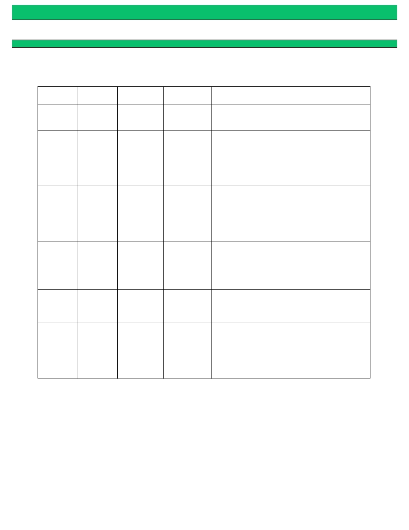
PIN DESCRIPTION
MB582A (Transmitter)
(Continued)
Pin no.
Symbol
Pin name
I/O interface
(speed)
Function
24, 23
20 to 17,
14,13
D0 to D7
Parallel data
input
TTL input
<19.44
Mbyte/s>
Parallel data input pins:
fetched at the rising edge of the PICLK pulse or by
the internal parallel clock.
Parallel data D0 to D7 are
10
PICLK
Parallel clock
input
TTL input
<19.44 MHz>
Clock input pin for parallel data fetching:
Parallel data D0 to D7 are fetched at the rising edge
of the PICLK pulse. This pin is used for the clock
synthesizer. Connect a stable oscillator (such as a
crystal oscillator within
±
20 ppm) to this pin. This pin
is used when PCLKSEL = “0”. This pin can’t be used
when REFSEL = “0”.
9
PCLKSEL
Parallel clock
selection
TTL input
<0 or 1>
Clock selection pin for parallel data fetching:
The internal parallel clock and PICLK are selected
when this pin inputs “1” and “0,” respectively.
Also, this pin is used to select the reference clock for
the clock synthesizer. REFCLK and PICLK are
selected when this pin inputs “1” and “0”,
respectively.
46
REFCLK
Reference
clock input
TTL input
<19.44 or
51.84 MHz>
Reference clock input pin:
PLL circuit in the clock synthesizer. Connect a
stable oscillator (such as a crystal oscillator within
±
20 ppm) to this pin.
One of two reference clocks can be selected.
This pin is used when PCLKSEL = “1”.
This pin is used for the
32
REFSEL
Reference
clock
selection
TTL input
<0 or 1>
Reference clock selection pin:
The 19.44- and 51.84-MHz reference clocks are
selected when this pin inputs “1” and “0,”
respectively.
4
EXTCLK
External
clock input
PECL input
<up to
155.52 MHz>
Single PECL input pin:
frequency external clock signal to execute an 8-to-1
multiplexer function independent of the clock
synthesizer.
In this case, the operating frequency is free and may
be up to 155.52 MHz. This pin is used when
CLKSEL = “0”.
This pin inputs a high-
相關PDF資料 |
PDF描述 |
|---|---|
| MB6021A | PCM Coders/Decoders(脈沖編碼器/解碼器) |
| MB60HXXX | CMOS Gate Array |
| MB61VHXXX | CMOS Gate Array |
| MB63HXXX | CMOS Gate Array |
| MB64HBXXX | CMOS Gate Array |
相關代理商/技術參數(shù) |
參數(shù)描述 |
|---|---|
| MB59 | 制造商:PANJIT 制造商全稱:Pan Jit International Inc. 功能描述:SURFACE MOUNT SCHOTTKY BARRIER RECTIFIER |
| MB59101BAN | 制造商:MURATA 制造商全稱:Murata Manufacturing Co., Ltd. 功能描述:HIGH FREQUENCY CERAMIC CAPACITORS |
| MB59101BBN | 制造商:MURATA 制造商全稱:Murata Manufacturing Co., Ltd. 功能描述:HIGH FREQUENCY CERAMIC CAPACITORS |
| MB59101CAN | 制造商:MURATA 制造商全稱:Murata Manufacturing Co., Ltd. 功能描述:HIGH FREQUENCY CERAMIC CAPACITORS |
| MB59101CBN | 制造商:MURATA 制造商全稱:Murata Manufacturing Co., Ltd. 功能描述:HIGH FREQUENCY CERAMIC CAPACITORS |
發(fā)布緊急采購,3分鐘左右您將得到回復。