- 您現(xiàn)在的位置:買賣IC網(wǎng) > PDF目錄377951 > MBM29LV200T (Fujitsu Limited) 2 M (256 K ×8/128 K ×16)Flash Memory((256 K ×8/128 K ×16) 單3V 電源電壓閃速存儲器) PDF資料下載
參數(shù)資料
| 型號: | MBM29LV200T |
| 廠商: | Fujitsu Limited |
| 英文描述: | 2 M (256 K ×8/128 K ×16)Flash Memory((256 K ×8/128 K ×16) 單3V 電源電壓閃速存儲器) |
| 中文描述: | 2米(256畝× 8 / 128畝× 16)閃存((256畝× 8 / 128畝× 16)單3V的電源電壓閃速存儲器) |
| 文件頁數(shù): | 15/51頁 |
| 文件大小: | 331K |
| 代理商: | MBM29LV200T |
第1頁第2頁第3頁第4頁第5頁第6頁第7頁第8頁第9頁第10頁第11頁第12頁第13頁第14頁當前第15頁第16頁第17頁第18頁第19頁第20頁第21頁第22頁第23頁第24頁第25頁第26頁第27頁第28頁第29頁第30頁第31頁第32頁第33頁第34頁第35頁第36頁第37頁第38頁第39頁第40頁第41頁第42頁第43頁第44頁第45頁第46頁第47頁第48頁第49頁第50頁第51頁
15
MBM29LV200T/MBM29LV200B
Notes:
1. Address bits A
15
to A
16
= X = “H” or “L” for all address commands except or Program Address (PA) and
sector Address (SA).
2. Bus operations are defined in Tables 2 and 3.
3. RA =Address of the memory location to be read.
PA =Address of the memory location to be programmed. Addresses are latched on the falling edge of
the WE pulse.
SA =Address of the sector to be erased. The combination of A
16
, A
15
, A
14
, A
13
, and A
12
will uniquely
select any sector.
4. RD =Data read from location RA during read operation.
PD =Data to be programmed at location PA. Data is latched on the falling edge of WE.
5. The system should generate the following address patterns:
Word Mode: 5555H or 2AAAH to addresses A
0
to A
14
Byte Mode: AAAAH or 5555H to addresses A
-1
and A
0
to A
14
6. Both Read/Reset commands are functionally equivalent, resetting the device to the read mode.
Command Definitions
Device operations are selected by writing specific address and data sequences into the command register.
Writing incorrect address and data values or writing them in the improper sequence will reset the devices to the
read mode. Table 7 defines the valid register command sequences. Note that the Erase Suspend (B0H) and
Erase Resume (30H) commands are valid only while the Sector Erase operation is in progress. Moreover both
Read/Reset commands are functionally equivalent, resetting the device to the read mode. Please note that
commands are always written at DQ
0
to DQ
7
and DQ
8
to DQ
15
bits are ignored.
Read/Reset Command
In order to return from Autoselect mode or Exceeded Timing Limits (DQ
5
= 1) to read/reset mode, the read/reset
operation is initiated by writing the read/reset command sequence into the command register. Microprocessor
read cycles retrieve array data from the memory. The devices remain enabled for reads until the command
register contents are altered.
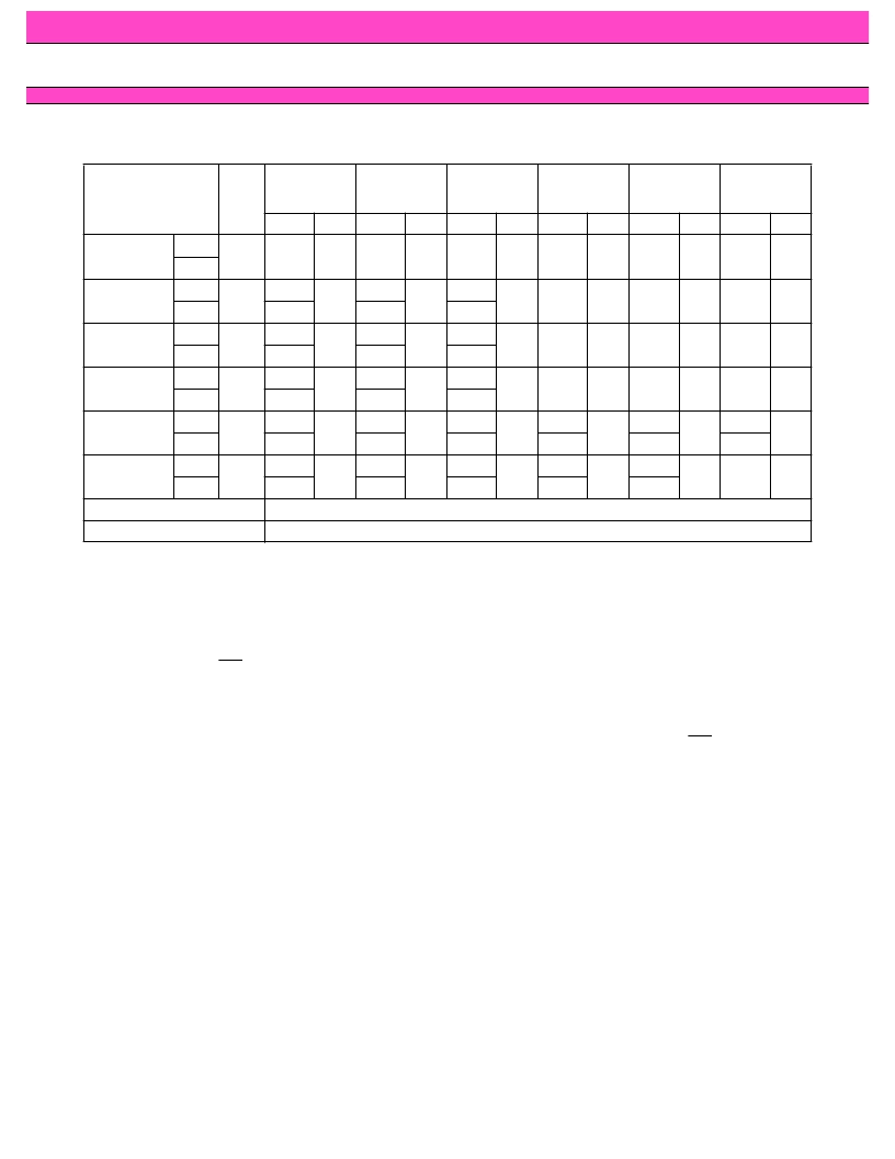
Table 7 MBM29LV200T/B Command Definitions
Command
Sequence
Bus
Write
Cycles
Req’d
First Bus
Write Cycle
Second
Bus
Write Cycle
Third Bus
Write Cycle
Fourth Bus
Read/Write
Cycle
Fifth Bus
Write Cycle
Sixth Bus
Write Cycle
Addr. Data Addr. Data Addr. Data Addr. Data Addr. Data Addr. Data
Read/Reset
Word
Byte
Word
Byte
Word
Byte
Word
Byte
Word
Byte
Word
Byte
1
XXXH F0H
—
—
—
—
—
—
—
—
—
—
Read/Reset
3
5555H
AAAH
5555H
AAAH
5555H
AAAH
5555H
AAAH
5555H
AAAH
Erase can be suspended during sector erase with Addr (“H” or “L”). Data (B0H)
Erase can be resumed after suspend with Addr (“H” or “L”). Data (30H)
AAH
2AAAH
5555H
2AAAH
5555H
2AAAH
5555H
2AAAH
5555H
2AAAH
5555H
55H
5555H
AAAH
5555H
AAAH
5555H
AAAH
5555H
AAAH
5555H
AAAH
F0H
RA
RD
—
—
—
—
Autoselect
3
AAH
55H
90H
—
—
—
—
—
—
Byte Program
4
AAH
55H
A0H
PA
PD
—
—
—
—
Chip Erase
6
AAH
55H
80H
5555H
AAAH
5555H
AAAH
AAH
2AAAH
5555H
2AAAH
5555H
55H
5555H
AAAH
10H
Sector Erase
6
AAH
55H
80H
AAH
55H
SA
30H
Sector Erase Suspend
Sector Erase Resume
相關(guān)PDF資料 |
PDF描述 |
|---|---|
| MBM29LV320BE | Triacs - I<sub>GT</sub>: 10 mA; I<sub>T</sub> (R<sub>MS</sub>): 1 A; V<sub>DRM</sub>: 800 V |
| MBM29LV320BE10TR | 32 M (4 M X 8/2 M X 16) BIT |
| MBM29LV320TE90 | 32 M (4 M X 8/2 M X 16) BIT |
| MBM29LV320TE90PBT | 32 M (4 M X 8/2 M X 16) BIT |
| MBM29LV320TE90TN | 32 M (4 M X 8/2 M X 16) BIT |
相關(guān)代理商/技術(shù)參數(shù) |
參數(shù)描述 |
|---|---|
| MBM29LV200TC | 制造商:FUJITSU 制造商全稱:Fujitsu Component Limited. 功能描述:2M (256K X 8/128K X 16) BIT |
| MBM29LV200TC-12 | 制造商:FUJITSU 制造商全稱:Fujitsu Component Limited. 功能描述:2M (256K X 8/128K X 16) BIT |
| MBM29LV200TC-12PFTN | 制造商:FUJITSU 制造商全稱:Fujitsu Component Limited. 功能描述:2M (256K X 8/128K X 16) BIT |
| MBM29LV200TC-12PFTR | 制造商:FUJITSU 制造商全稱:Fujitsu Component Limited. 功能描述:2M (256K X 8/128K X 16) BIT |
| MBM29LV200TC-70 | 制造商:FUJITSU 制造商全稱:Fujitsu Component Limited. 功能描述:2M (256K X 8/128K X 16) BIT |
發(fā)布緊急采購,3分鐘左右您將得到回復(fù)。