- 您現(xiàn)在的位置:買賣IC網(wǎng) > PDF目錄45211 > MC68331CPV20 (FREESCALE SEMICONDUCTOR INC) 32-BIT, 20.97 MHz, MICROCONTROLLER, PQFP144 PDF資料下載
參數(shù)資料
| 型號: | MC68331CPV20 |
| 廠商: | FREESCALE SEMICONDUCTOR INC |
| 元件分類: | 微控制器/微處理器 |
| 英文描述: | 32-BIT, 20.97 MHz, MICROCONTROLLER, PQFP144 |
| 封裝: | TQFP-144 |
| 文件頁數(shù): | 216/254頁 |
| 文件大?。?/td> | 1366K |
| 代理商: | MC68331CPV20 |
第1頁第2頁第3頁第4頁第5頁第6頁第7頁第8頁第9頁第10頁第11頁第12頁第13頁第14頁第15頁第16頁第17頁第18頁第19頁第20頁第21頁第22頁第23頁第24頁第25頁第26頁第27頁第28頁第29頁第30頁第31頁第32頁第33頁第34頁第35頁第36頁第37頁第38頁第39頁第40頁第41頁第42頁第43頁第44頁第45頁第46頁第47頁第48頁第49頁第50頁第51頁第52頁第53頁第54頁第55頁第56頁第57頁第58頁第59頁第60頁第61頁第62頁第63頁第64頁第65頁第66頁第67頁第68頁第69頁第70頁第71頁第72頁第73頁第74頁第75頁第76頁第77頁第78頁第79頁第80頁第81頁第82頁第83頁第84頁第85頁第86頁第87頁第88頁第89頁第90頁第91頁第92頁第93頁第94頁第95頁第96頁第97頁第98頁第99頁第100頁第101頁第102頁第103頁第104頁第105頁第106頁第107頁第108頁第109頁第110頁第111頁第112頁第113頁第114頁第115頁第116頁第117頁第118頁第119頁第120頁第121頁第122頁第123頁第124頁第125頁第126頁第127頁第128頁第129頁第130頁第131頁第132頁第133頁第134頁第135頁第136頁第137頁第138頁第139頁第140頁第141頁第142頁第143頁第144頁第145頁第146頁第147頁第148頁第149頁第150頁第151頁第152頁第153頁第154頁第155頁第156頁第157頁第158頁第159頁第160頁第161頁第162頁第163頁第164頁第165頁第166頁第167頁第168頁第169頁第170頁第171頁第172頁第173頁第174頁第175頁第176頁第177頁第178頁第179頁第180頁第181頁第182頁第183頁第184頁第185頁第186頁第187頁第188頁第189頁第190頁第191頁第192頁第193頁第194頁第195頁第196頁第197頁第198頁第199頁第200頁第201頁第202頁第203頁第204頁第205頁第206頁第207頁第208頁第209頁第210頁第211頁第212頁第213頁第214頁第215頁當(dāng)前第216頁第217頁第218頁第219頁第220頁第221頁第222頁第223頁第224頁第225頁第226頁第227頁第228頁第229頁第230頁第231頁第232頁第233頁第234頁第235頁第236頁第237頁第238頁第239頁第240頁第241頁第242頁第243頁第244頁第245頁第246頁第247頁第248頁第249頁第250頁第251頁第252頁第253頁第254頁
MOTOROLA
SYSTEM INTEGRATION MODULE
MC68331
4-22
USER’S MANUAL
4
The largest amount of data that can be transferred by a single bus cycle is an aligned
word. If the MCU transfers a long-word operand through a 16-bit port, the most signif-
icant operand word is transferred on the first bus cycle and the least significant oper-
and word is transferred on a following bus cycle.
4.4.5 Operand Transfer Cases
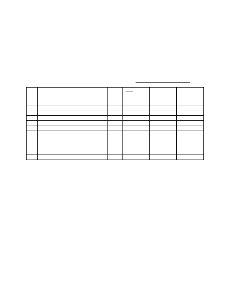
Table 4-13 is a summary of how operands are aligned for various types of transfers.
OPn entries are portions of a requested operand that are read or written during a bus
cycle and are defined by SIZ1, SIZ0, and ADDR0 for that bus cycle. The following
paragraphs discuss all the allowable transfer cases in detail.
4.5 Bus Operation
Internal microcontroller modules are typically accessed in two system clock cycles,
with no wait states. Regular external bus cycles use handshaking between the MCU
and external peripherals to manage transfer size and data. These accesses take three
system clock cycles, again with no wait states. During regular cycles, wait states can
be inserted as needed by bus control logic. Refer to 4.5.2 Regular Bus Cycles for
more information.
Fast-termination cycles, which are two-cycle external accesses with no wait states,
use chip-select logic to generate handshaking signals internally. Chip-select logic can
also be used to insert wait states before internal generation of handshaking signals.
Refer to 4.5.3 Fast Termination Cycles and 4.8 Chip Selects for more information.
Bus control signal timing, as well as chip-select signal timing, are specified in APPEN-
DIX A ELECTRICAL CHARACTERISTICS. Refer to the SIM Reference Manual (SIM-
RM/AD) for more information about each type of bus cycle.
The MCU is responsible for de-skewing signals it issues at both the start and the end
of a cycle. In addition, the MCU is responsible for de-skewing acknowledge and data
signals from peripheral devices.
1. The CPU32 does not support misaligned transfers.
2. Three-byte transfer cases occur only as a result of a long word to byte transfer.
Table 4-13 Operand Transfer Cases
Read Cycles
Write Cycles
Num
Transfer Case
SIZ
[1:0]
ADDR0 DSACK
[1:0]
DATA
[15:8]
DATA
[7:0]
DATA
[15:8]
DATA
[7:0]
Next
Cycle
1
Byte to 8-Bit Port (Even/Odd)
01
X
10
OP0
—
OP0
(OP0)
—
2
Byte to 16-Bit Port (Even)
01
0
01
OP0
—
OP0
(OP0)
—
3
Byte to 16-Bit Port (Odd)
01
1
01
—
OP0
(OP0)
OP0
—
4
Word to 8-Bit Port (Aligned)
10
0
10
OP0
—
OP0
(OP1)
1
5
Word to 8-Bit Port (Misaligned)1
10
1
10
OP0
—
OP0
(OP0)
1
6
Word to 16-Bit Port (Aligned)
10
0
11
OP0
OP1
OP0
OP1
—
7
Word to 16-Bit Port (Misaligned)1
10
1
01
—
OP0
(OP0)
OP0
2
8
Long Word to 8-Bit Port (Aligned)
00
0
10
OP0
—
OP0
(OP1)
13
9
Long Word to 8-Bit Port (Misaligned)1
10
1
10
OP0
—
OP0
(OP0)
12
10
Long Word to 16-Bit Port (Aligned)
00
0
01
OP0
OP1
OP0
OP1
6
11
Long Word to 16-Bit Port (Misaligned)1
10
1
01
—
OP0
(OP0)
OP0
2
12
3 Byte to 8-Bit Port (Aligned)2
11
0
10
OP0
—
OP0
(OP1)
5
13
3 Byte to 8-Bit Port (Misaligned)2
11
1
10
OP0
—
OP0
(OP0)
4
相關(guān)PDF資料 |
PDF描述 |
|---|---|
| MC68331CFC25 | 32-BIT, MICROCONTROLLER, PQFP132 |
| MC68331MFC16 | 32-BIT, 16.78 MHz, MICROCONTROLLER, PQFP132 |
| MC68331CFC16 | 32-BIT, 16.78 MHz, MICROCONTROLLER, PQFP132 |
| MC68332GCPV16 | 32-BIT, 16.78 MHz, MICROCONTROLLER, PQFP144 |
| MC68332GVPV25 | 32-BIT, 25 MHz, MICROCONTROLLER, PQFP144 |
相關(guān)代理商/技術(shù)參數(shù) |
參數(shù)描述 |
|---|---|
| MC68331CPV20B1 | 制造商:Rochester Electronics LLC 功能描述:32BIT MCU,GPT,SIM,QSM - Bulk |
| MC68331CPV25 | 制造商:Rochester Electronics LLC 功能描述:32BIT MCU,GPT,SIM,QSM - Bulk |
| MC68331LPV20 | 制造商:Motorola Inc 功能描述: |
| MC68331MEH16 | 功能描述:32位微控制器 - MCU 32B MCU GPT SIM QSM RoHS:否 制造商:Texas Instruments 核心:C28x 處理器系列:TMS320F28x 數(shù)據(jù)總線寬度:32 bit 最大時鐘頻率:90 MHz 程序存儲器大小:64 KB 數(shù)據(jù) RAM 大小:26 KB 片上 ADC:Yes 工作電源電壓:2.97 V to 3.63 V 工作溫度范圍:- 40 C to + 105 C 封裝 / 箱體:LQFP-80 安裝風(fēng)格:SMD/SMT |
| MC68331MFC16 | 制造商:MOTOROLA 制造商全稱:Motorola, Inc 功能描述:User’s Manual |
發(fā)布緊急采購,3分鐘左右您將得到回復(fù)。