- 您現(xiàn)在的位置:買賣IC網(wǎng) > PDF目錄377972 > ML674000 (OKI SEMICONDUCTOR CO., LTD.) CMOS 32-Bit ARM-Based General-Purpose Single-Chip Microcontroller(基于ARM的32位CMOS單片機) PDF資料下載
參數(shù)資料
| 型號: | ML674000 |
| 廠商: | OKI SEMICONDUCTOR CO., LTD. |
| 英文描述: | CMOS 32-Bit ARM-Based General-Purpose Single-Chip Microcontroller(基于ARM的32位CMOS單片機) |
| 中文描述: | 的CMOS 32位基于ARM通用單芯片微控制器(基于ARM公司的32位的CMOS單片機) |
| 文件頁數(shù): | 8/42頁 |
| 文件大小: | 529K |
| 代理商: | ML674000 |
第1頁第2頁第3頁第4頁第5頁第6頁第7頁當前第8頁第9頁第10頁第11頁第12頁第13頁第14頁第15頁第16頁第17頁第18頁第19頁第20頁第21頁第22頁第23頁第24頁第25頁第26頁第27頁第28頁第29頁第30頁第31頁第32頁第33頁第34頁第35頁第36頁第37頁第38頁第39頁第40頁第41頁第42頁
PEDL674000-02
OKI Semiconductor
ML674000
6/38
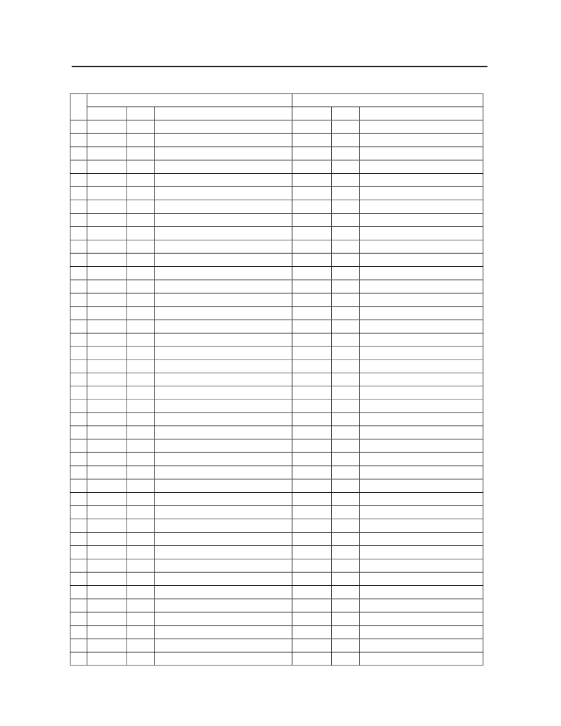
Primary Function
Secondary Function
Pin
Symbol
Type
Description
Symbol
Type
Description
80
81
82
GND_CORE
GND
83
VDD_CORE
VDD
84
XA[13]
85
XA[14]
86
XA[15]
87
XA[16]
88
XA[17]
89
GND_IO
90
XA[18]
91
PIOA[10]
92
PIOA[11]
93
PIOA[12]
94
VDD_IO
95
PIOA[13]
96
PIOA[14]
97
PIOA[15]
98
XOE_N
99
XWE_N
100
GND_IO
101
XBWE_N[0]
102
XBWE_N[1]
103
XROMCS_N
104
XRAMCS_N
105
XIOCS_N[0]
106
XIOCS_N[1]
107
GND_CORE
GND
108
VDD_CORE
VDD
109
PIOB[0]
110
PIOB[1]
111
VDD_IO
112
PIOB[2]
113
PIOB[3]
114
PIOB[4]
115
PIOB[5]
116
GND_IO
117
PIOB[6]
118
PIOB[7]
119
XBS_N[0]
120
XBS_N[1]
XA[11]
O
O
External memory access address output port
—
XA[12]
External memory access address output port
—
GND for CORE
—
Power supply for CORE
—
O
O
O
O
O
O
O
I/O
I/O
I/O
VDD
I/O
I/O
I/O
O
O
GND
O
O
O
O
O
O
External memory access address output port
—
External memory access address output port
—
External memory access address output port
—
External memory access address output port
—
External memory access address output port
—
GND for I/O
—
External memory access address output port
—
General port (with interrupt function)
XA[19]
O
O
O
External memory access address output port
General port (with interrupt function)
XA[20]
External memory access address output port
General port (with interrupt function)
XA[21]
External memory access address output port
Power supply for I/O
General port (with interrupt function)
XA[22]
O
O
O
External memory access address output port
General port (with interrupt function)
XA[23]
External memory access address output port
General port (with interrupt function)
XWR
Transfer direction of external bus
Output enable (excluding SDRAM)
—
Write enable
—
GND for I/O
Byte write enable (LSB)
—
Byte write enable (MSB)
—
External ROM chip select
—
External RAM chip select
—
IO bank 0 chip select
—
IO bank 1 chip select
—
GND for CORE
—
Power supply for CORE
—
I/O
I/O
VDD
I/O
I/O
I/O
I/O
GND
I/O
I/O
O
O
General port (with interrupt function)
DREQ0
I
DMA request signal (CH0)
General port (with interrupt function)
DREQCLR0
O
DREQ clear signal (CH0)
Power supply for I/O
—
General port (with interrupt function)
DREQ1
I
DMA request signal (CH1)
General port (with interrupt function)
DREQCLR1
O
O
O
DREQ clear signal (CH1)
General port (with interrupt function)
TCOUT0
DMAC Terminal Count (CH0)
General port (with interrupt function)
TCOUT1
DMAC Terminal Count (CH1)
GND for I/O
—
General port (with interrupt function)
PWMOUT[0]
O
O
PWM output (CH0)
General port (with interrupt function)
PWMOUT[1]
PWM output (CH1)
External bus byte select (LSB)
—
External bus byte select (MSB)
—
相關PDF資料 |
PDF描述 |
|---|---|
| ML67Q4003 | 32-bit ARM-Based General-Purpose Microcontroller(32位ARM通用微控制器) |
| ML7000 | PCM Voice Codec(PCM話音編碼譯碼器) |
| ML7001 | PCM Voice Codec(PCM話音編碼譯碼器) |
| ML7001-01 | Single Rail CODEC |
| ML7001-02 | Single Rail CODEC |
相關代理商/技術參數(shù) |
參數(shù)描述 |
|---|---|
| ML674000-KIT | 制造商:ROHM Semiconductor 功能描述:CMOS 32-Bit ARM-Based General-Purpose Single-Chip Microcontroller |
| ML674000LA | 制造商:ROHM Semiconductor 功能描述:ML674000LAZ03A |
| ML674000LAZ03A-7 | 制造商:ROHM Semiconductor 功能描述:NEW PART NO ML674000LAZ0ARL 制造商:ROHM Semiconductor 功能描述:ML674000LAZ03A-7 - Bulk |
| ML674000LAZ0AL | 制造商:ROHM Semiconductor 功能描述:ML674000LAZ0AL - Bulk |
| ML674000TBZ03A-7 | 制造商:ROHM Semiconductor 功能描述:Integrated Dual UART ARM7TDMI MCU 制造商:ROHM Semiconductor 功能描述:ARM7TDMI microprocessor integrated dual UART |
發(fā)布緊急采購,3分鐘左右您將得到回復。