- 您現(xiàn)在的位置:買賣IC網(wǎng) > PDF目錄359218 > MRF6S19100HR3 (飛思卡爾半導體(中國)有限公司) RF Power Field Effect Transistors PDF資料下載
參數(shù)資料
| 型號: | MRF6S19100HR3 |
| 廠商: | 飛思卡爾半導體(中國)有限公司 |
| 英文描述: | RF Power Field Effect Transistors |
| 中文描述: | 射頻功率場效應(yīng)晶體管 |
| 文件頁數(shù): | 1/12頁 |
| 文件大?。?/td> | 398K |
| 代理商: | MRF6S19100HR3 |
MRF6S19100HR3 MRF6S19100HSR3
1
RF Device Data
Freescale Semiconductor
RF Power Field Effect Transistors
N-Channel Enhancement-Mode Lateral MOSFETs
Designed for N-CDMA base station applications with frequencies from 1930
to 1990 MHz. Suitable for TDMA, CDMA and multicarrier amplifier applica-
tions. To be used in Class AB for PCN - PCS/cellular radio and WLL
applications.
Typical 2-Carrier N-CDMA Performance: V
DD
= 28 Volts, I
DQ
= 900 mA,
P
out
= 22 Watts Avg., Full Frequency Band, IS-95 (Pilot, Sync, Paging,
Traffic Codes 8 Through 13) Channel Bandwidth = 1.2288 MHz. PAR =
9.8 dB @ 0.01% Probability on CCDF.
Power Gain — 16.1 dB
Drain Efficiency — 28%
IM3 @ 2.5 MHz Offset — -37 dBc @ 1.2288 MHz Channel Bandwidth
ACPR @ 885 kHz Offset — -51 dBc @ 30 kHz Channel Bandwidth
Capable of Handling 10:1 VSWR, @ 28 Vdc, 1960 MHz, 100 Watts CW
Output Power
Characterized with Series Equivalent Large-Signal Impedance Parameters
Internally Input and Output Matched for Ease of Use
Qualified Up to a Maximum of 32 V
DD
Operation
Integrated ESD Protection
Lower Thermal Resistance Package
Designed for Lower Memory Effects and Wide Instantaneous Bandwidth
Applications
Low Gold Plating Thickness on Leads, 40
μ″
Nominal.
Pb-Free and RoHS Compliant
In Tape and Reel. R3 Suffix = 250 Units per 56 mm, 13 inch Reel.
Table 1. Maximum Ratings
Rating
Symbol
Value
Unit
Drain-Source Voltage
V
DSS
-0.5, +68
Vdc
Gate-Source Voltage
V
GS
-0.5, +12
Vdc
Total Device Dissipation @ T
C
= 25
°
C
Derate above 25
°
C
P
D
398
2.3
W
W/
°
C
Storage Temperature Range
T
stg
- 65 to +150
°
C
Operating Junction Temperature
T
J
200
°
C
CW Operation
CW
100
W
Table 2. Thermal Characteristics
Characteristic
Symbol
Value
(1,2)
Unit
Thermal Resistance, Junction to Case
Case Temperature 80
°
C, 100 W CW
Case Temperature 77
°
C, 22 W CW
R
θ
JC
0.44
0.50
°
C/W
1. MTTF calculator available at http://www.freescale.com/rf. Select Tools/Software/Application Software/Calculators to access
the MTTF calculators by product.
2. Refer to AN1955,
Thermal Measurement Methodology of RF Power Amplifiers.
Go to http://www.freescale.com/rf.
Select Documentation/Application Notes - AN1955.
NOTE -
CAUTION
- MOS devices are susceptible to damage from electrostatic charge. Reasonable precautions in handling and
packaging MOS devices should be observed.
Document Number: MRF6S19100H
Rev. 3, 8/2005
Freescale Semiconductor
Technical Data
MRF6S19100HR3
MRF6S19100HSR3
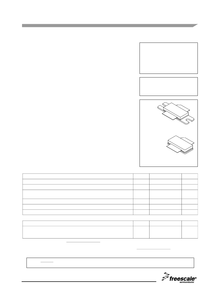
1990 MHz, 22 W AVG., 28 V
2 x N-CDMA
LATERAL N-CHANNEL
RF POWER MOSFETs
CASE 465A-06, STYLE 1
NI-780S
MRF6S19100HSR3
CASE 465-06, STYLE 1
NI-780
MRF6S19100HR3
Freescale Semiconductor, Inc., 2005. All rights reserved.
相關(guān)PDF資料 |
PDF描述 |
|---|---|
| MRF6S19140HR3 | N-Channel Enhancement-Mode Lateral MOSFETs |
| MRF6S19140HSR3 | N-Channel Enhancement-Mode Lateral MOSFETs |
| MRF6S20010GNR1 | RF Power Field Effect Transistors |
| MRF6S21050LR3 | RF Power Field Effect Transistors |
| MRF6S21050LSR3 | RF Power Field Effect Transistors |
相關(guān)代理商/技術(shù)參數(shù) |
參數(shù)描述 |
|---|---|
| MRF6S19100HR3_06 | 制造商:FREESCALE 制造商全稱:Freescale Semiconductor, Inc 功能描述:RF Power Field Effect Transistors N-Channel Enhancement-Mode Lateral MOSFETs |
| MRF6S19100HR3_08 | 制造商:FREESCALE 制造商全稱:Freescale Semiconductor, Inc 功能描述:RF Power Field Effect Transistors N-Channel Enhancement-Mode Lateral MOSFETs |
| MRF6S19100HR5 | 功能描述:射頻MOSFET電源晶體管 HV6 WCDMA 22W NI780H RoHS:否 制造商:Freescale Semiconductor 配置:Single 晶體管極性: 頻率:1800 MHz to 2000 MHz 增益:27 dB 輸出功率:100 W 汲極/源極擊穿電壓: 漏極連續(xù)電流: 閘/源擊穿電壓: 最大工作溫度: 封裝 / 箱體:NI-780-4 封裝:Tray |
| MRF6S19100HS | 制造商:Freescale Semiconductor 功能描述: |
| MRF6S19100HSR3 | 功能描述:射頻MOSFET電源晶體管 HV6 WCDMA 22W NI780HS RoHS:否 制造商:Freescale Semiconductor 配置:Single 晶體管極性: 頻率:1800 MHz to 2000 MHz 增益:27 dB 輸出功率:100 W 汲極/源極擊穿電壓: 漏極連續(xù)電流: 閘/源擊穿電壓: 最大工作溫度: 封裝 / 箱體:NI-780-4 封裝:Tray |
發(fā)布緊急采購,3分鐘左右您將得到回復(fù)。