- 您現(xiàn)在的位置:買賣IC網(wǎng) > PDF目錄383639 > MS27C801 (意法半導(dǎo)體) 8 Mbit (1Mb x 8) UV EPROM and OTP EPROM PDF資料下載
參數(shù)資料
| 型號: | MS27C801 |
| 廠商: | 意法半導(dǎo)體 |
| 英文描述: | 8 Mbit (1Mb x 8) UV EPROM and OTP EPROM |
| 中文描述: | 8兆(1兆× 8)紫外線存儲器和OTP存儲器 |
| 文件頁數(shù): | 5/16頁 |
| 文件大?。?/td> | 158K |
| 代理商: | MS27C801 |
5/16
M27C801
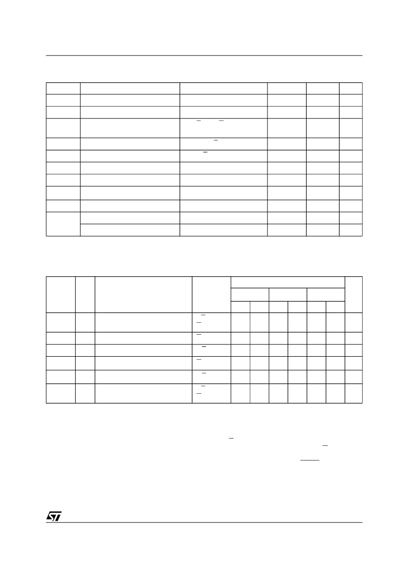
Table 7. Read Mode DC Characteristics
(1)
(T
A
= 0 to 70 °C or –40 to 85 °C; V
CC
= 5V ± 10%)
Symbol
Parameter
Note: 1. V
CC
must be applied simultaneously with or before V
PP
and removed simultaneously or after V
PP
.
2. Maximum DC voltage on Output is V
CC
+0.5V.
Table 8A. Read Mode AC Characteristics
(1)
(T
A
= 0 to 70 °C or –40 to 85 °C; V
CC
= 5V ± 10%)
Note: 1. V
CC
must be applied simultaneously with or before V
PP
and removed simultaneously or after V
PP.
2. Sampled only, not 100% tested.
3. Speed obtained with High Speed AC measurement conditions.
Test Condition
Min
Max
Unit
I
LI
Input Leakage Current
0V
≤
V
IN
≤
V
CC
±10
μ
A
I
LO
Output Leakage Current
0V
≤
V
OUT
≤
V
CC
±10
μ
A
I
CC
Supply Current
E = V
IL
, GV
PP
= V
IL
,
I
OUT
= 0mA, f = 5MHz
35
mA
I
CC1
Supply Current (Standby) TTL
E = V
IH
1
mA
I
CC2
Supply Current (Standby) CMOS
E > V
CC
– 0.2V
100
μ
A
I
PP
Program Current
V
PP
= V
CC
10
μ
A
V
IL
Input Low Voltage
–0.3
0.8
V
V
IH
(2)
Input High Voltage
2
V
CC
+ 1
V
V
OL
Output Low Voltage
I
OL
= 2.1mA
0.4
V
V
OH
Output High Voltage TTL
I
OH
= –1mA
3.6
V
Output High Voltage CMOS
I
OH
= –100
μ
A
V
CC
– 0.7
V
Symbol
Alt
Parameter
Test
Condition
M27C801
Unit
-45
(3)
-60
-70
Min
Max
Min
Max
Min
Max
t
AVQV
t
ACC
Address Valid to Output Valid
E = V
IL
,
GV
PP
= V
IL
45
60
70
ns
t
ELQV
t
CE
Chip Enable Low to Output Valid
GV
PP
= V
IL
45
60
70
ns
t
GLQV
t
OE
Output Enable Low to Output Valid
E = V
IL
25
30
35
ns
t
EHQZ (2)
t
DF
Chip Enable High to Output Hi-Z
GV
PP
= V
IL
0
25
0
25
0
30
ns
t
GHQZ (2)
t
DF
Output Enable High to Output Hi-Z
E = V
IL
0
25
0
25
0
30
ns
t
AXQX
t
OH
Address Transition to Output
Transition
E = V
IL
,
GV
PP
= V
IL
0
0
0
ns
Two Line Output Control
Because EPROMs are usually used in larger
memory arrays, the product features a 2 line con-
trol function which accommodates the use of mul-
tiple memory connection. The two line control
function allows:
a. the lowest possible memory power dissipation,
b. complete assurance that output bus contention
will not occur.
For the most efficient use of these two control
lines, E should be decoded and used as the prima-
ry device selecting function, while G should be
made a common connection to all devices in the
array and connected to the READ line from the
system control bus. This ensures that all deselect-
ed memory devices are in their low power standby
mode and that the output pins are only active
when data is required from a particular memory
device.
相關(guān)PDF資料 |
PDF描述 |
|---|---|
| MSC2712YT1 | General Purpose Amplifier Transistor |
| MSC2712GT1 | General Purpose Amplifier Transistors(通用放大晶體管) |
| MSD42SWT1 | NPN Silicon General Purpose High Voltage Transistor |
| MSD42SWT1G | NPN Silicon General Purpose High Voltage Transistor |
| MSOP8 | Motor Driver IC; No. of Drivers:2; Output Current Max:3A; Package/Case:44-PLCC; Leaded Process Compatible:Yes; Output Current Min:-3A; Peak Reflow Compatible (260 C):Yes; Mounting Type:Surface Mount; Voltage Rating:7V RoHS Compliant: Yes |
相關(guān)代理商/技術(shù)參數(shù) |
參數(shù)描述 |
|---|---|
| MS27-R | 制造商:TURCK Inc 功能描述:M0508412 |
| MS28005-3 | 制造商: 功能描述: 制造商:MILITARY STANDARDS PROMUL 功能描述: 制造商:undefined 功能描述: |
| MS28034-3 | 制造商:Contact Us 功能描述: |
| MS280536 | 制造商:Talley 功能描述:MS280536 |
| MS281 | 制造商:未知廠家 制造商全稱:未知廠家 功能描述:Power Film Resistors |
發(fā)布緊急采購,3分鐘左右您將得到回復(fù)。