- 您現(xiàn)在的位置:買賣IC網(wǎng) > PDF目錄69038 > MSM6242BGS-K (LAPIS SEMICONDUCTOR CO LTD) 0 TIMER(S), REAL TIME CLOCK, PDSO24 PDF資料下載
參數(shù)資料
| 型號: | MSM6242BGS-K |
| 廠商: | LAPIS SEMICONDUCTOR CO LTD |
| 元件分類: | 時(shí)鐘/數(shù)據(jù)恢復(fù)及定時(shí)提取 |
| 英文描述: | 0 TIMER(S), REAL TIME CLOCK, PDSO24 |
| 封裝: | 0.430 INCH, 1.27 MM PITCH, PLASTIC, SOP-24 |
| 文件頁數(shù): | 3/24頁 |
| 文件大小: | 293K |
| 代理商: | MSM6242BGS-K |
10/23
OKI Semiconductor
MSM6242B
FEDL6242B-02
Name
Pin No.
Description
PIN DESCRIPTION
GS-K
RS
D0
D1
D2
D3
A0
A1
A2
A3
ALE
WR
RD
CS0
XT
STD.P
VDD
GND
CS1
14
13
12
11
4
5
6
7
3
10
8
2
15
1
16
17
18
9
19
16
15
14
5
7
9
10
4
13
11
20
22
23
24
12
2
1
Data Input/Output pins to be directly connected to a microcontroller bus for
reading and writing of the clock/calendar's registers and control registers. D0 = LSB
and D3 = MSB.
Address input pin for use by a microcomputer to select internal clock/calendar's
registers and control registers for Read/Write operations (See Function Table
Figure 1). Address input pins A0-A3 are used in combination with ALE for
addressing registers.
Address Latch Enable pin. This pin enables writing of address data when ALE = 1
and CS0 = 0; address data is latched when ALE = 0 Microcontroller/Micro-
processors having an ALE output should connect to this pin; otherwise it should
be connected at VDD
Writing of data is performed by this pin.
When CS1 = 1 and CS0 = 0, D0 to D3 data is written into the register at the rising
edge of WR.
Reading of register data is accomplished using this pin. When CS1 = 1, CS0 = 0
and RD = 0, the data of this register is output to D0 to D3. If both RD and WR are
set at 0 simaltaneously, RD is to be inhibited.
Chip Select pins. These pins enable/disable ALE, RD and WR operation. CS0
and ALE work in combination with one another, while CS1 work independent
with ALE. CS1 must be connected to power failure detection as shown in Figure
18.
Output pin of N-CH OPEN DRAIN type. The output data is controlled by the
D1 data content of CE register. This pin has a priority to CS0 and CS1.
Refer to Figure 9 and FUNCTIONAL DESCRIPTION OF REGISTERS.
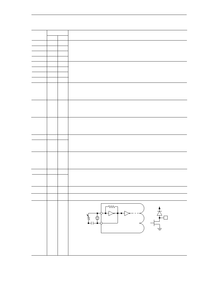
32.768 kHz crystal is to be connected to these pins.
When an external clock of 32.768 kHz is to be used for MSM6242B's oscillation
source, either CMOS output or pull-up TTL output is to be input from XT, while
XT should be left open.
Power supply pin. +2 to +6 V power is to be applied to this pin.
Ground pin.
VDD
STD.P OUTPUT
N-CH
RFB 5 MW
32.768 kHz
XT
VDD or GND
C1
C2
X'tal
XT
C1 = C2 = 15 to 30 pF
The impedance of the crystal should be less than 30 k
W
Figure 8 Oscillator Circuit
Figure 9
相關(guān)PDF資料 |
PDF描述 |
|---|---|
| MSM6242BRS | 0 TIMER(S), REAL TIME CLOCK, PDIP18 |
| MSM6255GS-V1K | 128 X 256 CHARACTERS DOT MAT LCD DSPL CTLR, PQFP80 |
| MSM62X42BGS-1K-S | REAL TIME CLOCK, PDSO24 |
| MSM63182-XXXGS-K | 4-BIT, MROM, 2 MHz, MICROCONTROLLER, PQFP128 |
| MSM63184B-XXXGS-K | 4-BIT, MROM, 2 MHz, MICROCONTROLLER, PQFP128 |
相關(guān)代理商/技術(shù)參數(shù) |
參數(shù)描述 |
|---|---|
| MSM6242BGS-KR1 | 制造商:ROHM Semiconductor 功能描述: |
| MSM6242BRS | 制造商:ROHM Semiconductor 功能描述: 制造商:OK International 功能描述: |
| MSM6242BRS-7 | 制造商:ROHM Semiconductor 功能描述:Directly connected to the bus real-time clock |
| MSM6250 | 制造商:QUALCOMM 制造商全稱:QUALCOMM 功能描述:CHIPSET SOLUTION |
| MSM6252 | 制造商:OKI 制造商全稱:OKI electronic componets 功能描述:64words X Bit FIFO |
發(fā)布緊急采購,3分鐘左右您將得到回復(fù)。