- 您現(xiàn)在的位置:買(mǎi)賣(mài)IC網(wǎng) > PDF目錄359235 > MT90840AL (ZARLINK SEMICONDUCTOR INC) Distributed Hyperchannel Switch PDF資料下載
參數(shù)資料
| 型號(hào): | MT90840AL |
| 廠商: | ZARLINK SEMICONDUCTOR INC |
| 元件分類(lèi): | 路由/交換 |
| 英文描述: | Distributed Hyperchannel Switch |
| 中文描述: | TELECOM, DIGITAL TIME SWITCH, PQFP100 |
| 封裝: | 14 X 20 MM, 2.80 MM HEIGHT, MO-112CC-1, MQFP-100 |
| 文件頁(yè)數(shù): | 26/51頁(yè) |
| 文件大小: | 512K |
| 代理商: | MT90840AL |
第1頁(yè)第2頁(yè)第3頁(yè)第4頁(yè)第5頁(yè)第6頁(yè)第7頁(yè)第8頁(yè)第9頁(yè)第10頁(yè)第11頁(yè)第12頁(yè)第13頁(yè)第14頁(yè)第15頁(yè)第16頁(yè)第17頁(yè)第18頁(yè)第19頁(yè)第20頁(yè)第21頁(yè)第22頁(yè)第23頁(yè)第24頁(yè)第25頁(yè)當(dāng)前第26頁(yè)第27頁(yè)第28頁(yè)第29頁(yè)第30頁(yè)第31頁(yè)第32頁(yè)第33頁(yè)第34頁(yè)第35頁(yè)第36頁(yè)第37頁(yè)第38頁(yè)第39頁(yè)第40頁(yè)第41頁(yè)第42頁(yè)第43頁(yè)第44頁(yè)第45頁(yè)第46頁(yè)第47頁(yè)第48頁(yè)第49頁(yè)第50頁(yè)第51頁(yè)
MT90840
Data Sheet
2-256
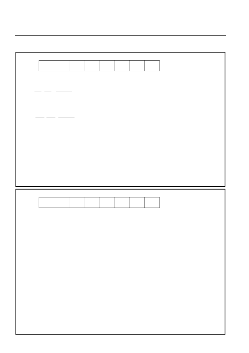
Register Description
Interface Mode Selection Register (IMS) - READ/WRITE
7
6
5
4
3
2
1
0
DR1
DR0
PPS1
PPS0
ODE
0
0
FDC
DR1-0
Serial Port Data Rate Selection. Select one of three different data rates at the serial inputs and outputs of the
MT90840.
DR1 DR0
0
0
1
1
Data Rate
2.048 Mbps
4.096 Mbps
8.192 Mbps
reserved
0
1
0
1
PPS1-0
Parallel Port Data Rate Selection. Select one of three different data rates for the parallel port of the MT90840.
PPS1 PPS0
0
0
1
1
Data Rate
reserved. Do not use.
6.480 Mbyte/s.
19.44 Mbyte/s.
16.384 Mbyte/s.
0
1
0
1
ODE
Output Drive Enable. When LOW, forces the MT90840 output-buffers on the serial and parallel data ports into the
high impedance state (STo0-STo7, STi0-STi7, and PDo0-7). If this output is HIGH, all channels have their output
drive enable controlled by the per-channel OE bits of Transmit Connection Memory High, or Receive Connection
Memory High.
FDC
Full Direction Control. This bit should only be set HIGH at the 2.048 Mbps serial rate. When FDC is set HIGH, each
time slot on each of the 16 ST-BUS pins can be individually configured as input or output. Up to 512 serial channels
can be “inserted” onto the Transmit parallel port, or up to 512 parallel channels can be “dropped” to the serial port.
Individual channel direction is controlled by the DC bits in the RPCM High. When FDC is LOW, the number of input
and output time slots are “balanced”, and setting a nominal input to be an output causes the same-number output
time slot on the same-number STo pin to become an input. For applications at 4.096 and 8.192 Mbps, this bit should
be LOW.
Note
: Bits 1 & 2 must be set to 0 by the CPU.
TM1-0
Timing Mode control bits. Define the four different timing modes described in the Timing and Switching Control
section.
0 0
0 1
1 0
1 1
Timing Mode 1
Timing Mode 2
Timing Mode 3
Timing Mode 4
C4/8R
C4/8R Input Reference Select. If set high, this bit enables the 4.096 or 8.192 MHz serial port reference clock to be
taken from input pin C4/8R1. If LOW, the reference is taken from input pin C4/8R2 (default).
TCP
Parallel Port Transmit Clock Polarity. To allow the MT90840 parallel port transmit clock to comply with different 155
Mbps framer backplanes, TCP controls which edge of the clock is used to transmit data at the parallel port. (The
clock is PCKT in TM1 or PCKR in TM2, 3, & 4). The TCP bit allows the rising (TCP=LOW) or the falling (TCP=HIGH)
edges of the transmit clock to be selected.
INTCLK
Internal 4.096 MHz Clock Divider. For use in TM2, in 19.44 or 16.384 MHz parallel-port applications. This bit controls
the operation of the internal clock divider driven by PCKR. When INTCLK is set HIGH the internal 4.096 MHz clock
(and the SPCKo output) are generated by dividing down the PCKR clock. When INTCLK is set LOW, the C4/8R bit
controls the source for the serial clock reference. In TM3 and TM4 the MT90840 automatically sets itself in the
internal divider mode and the state of INTCLK has no effect. In TM1 this bit is must be set LOW.
SFDI
Serial Frame Pulse Direction Control. Normally LOW, unless it is necessary to operate multiple parallel MT90840
devices in Timing Mode 2. When set HIGH, the F0 line becomes an input and this MT90840 is synchronized to the
timing of another MT90840 generating the F0o, and using the same 4.096 or 8.192 MHz reference input. One
MT90840 in TM2 with SFDI LOW can control several MT80940s with SFDI HIGH. When SFDI is set HIGH, INTCLK
is ignored, and SPFP in the GPM register must be set to the expected F0i polarity.
PFDI
Parallel Frame Pulse Direction Control. Normally LOW, unless it is necessary to operate multiple parallel MT90840
devices in Timing Mode 1. When set HIGH, the PPFT pin becomes an input and this MT90840 is synchronized to the
timing of another MT90840 generating the PPFTo. One MT90840 in TM1 with PFDI LOW can control several
MT80940s with PFDI HIGH. When PFDI is HIGH, PPFP in the GPM register must be set to the expected PPFTi
polarity.
Note
: Bit 7 must be set to 0 by the CPU.
Timing Mode Register (TIM) - READ/WRITE
7
6
5
4
3
2
1
0
TM1
TM0
C4/8R
TCP
INTCLK
SFDI
PFDI
0
相關(guān)PDF資料 |
PDF描述 |
|---|---|
| MT90866AG2 | Flexible 4 K x 2.4 K Channel Digital Switch with H.110 Interface and 2.4 K x 2.4 K Local Switch |
| MT90869 | Flexible 16K Digital Switch (F16kDX) |
| MT90869AG | Flexible 16K Digital Switch (F16kDX) |
| MT90870 | Flexible 12 k Digital Switch (F12kDX) |
| MT90871AV | Flexible 8K Digital Switch (F8KDX) |
相關(guān)代理商/技術(shù)參數(shù) |
參數(shù)描述 |
|---|---|
| MT90840AL1 | 制造商:Microsemi Corporation 功能描述:SWIT FABRIC 512 X 2430/512 X 512/2.373K X 2.373K 5V 100MQFP - Trays 制造商:MICROSEMI CONSUMER MEDICAL PRODUCT GROUP 功能描述:IC DGTL SWITCH DHS 100MQFP 制造商:Microsemi Corporation 功能描述:IC DGTL SWITCH DHS 100MQFP |
| MT90840AP | 制造商:Microsemi Corporation 功能描述:SWIT FABRIC 512 X 2430/512 X 512/2.373K X 2.373K 5V 84PLCC - Rail/Tube |
| MT90840AP1 | 制造商:Microsemi Corporation 功能描述:SWIT FABRIC 512 X 2430/512 X 512/2.373K X 2.373K 5V 84PLCC - Rail/Tube 制造商:MICROSEMI CONSUMER MEDICAL PRODUCT GROUP 功能描述:IC DGTL SWITCH DHS 84PLCC 制造商:Microsemi Corporation 功能描述:IC DGTL SWITCH DHS 84PLCC |
| MT90840APR1 | 制造商:Microsemi Corporation 功能描述:SWIT FABRIC 512 X 2430/512 X 512/2.373K X 2.373K 5V 84PLCC - Tape and Reel 制造商:MICROSEMI CONSUMER MEDICAL PRODUCT GROUP 功能描述:IC DGTL SWITCH DHS 84PLCC 制造商:Microsemi Corporation 功能描述:IC DGTL SWITCH DHS 84PLCC |
| MT9085 | 制造商:MITEL 制造商全稱:Mitel Networks Corporation 功能描述:CMOS PAC - Parallel Access Circuit |
發(fā)布緊急采購(gòu),3分鐘左右您將得到回復(fù)。