- 您現(xiàn)在的位置:買賣IC網(wǎng) > PDF目錄11733 > ORSO82G5-2FN680C (Lattice Semiconductor Corporation)IC TRANCEIVERS FPSC 680FPBGA PDF資料下載
參數(shù)資料
| 型號: | ORSO82G5-2FN680C |
| 廠商: | Lattice Semiconductor Corporation |
| 文件頁數(shù): | 101/153頁 |
| 文件大小: | 0K |
| 描述: | IC TRANCEIVERS FPSC 680FPBGA |
| 產(chǎn)品變化通告: | Product Discontinuation 01/Aug/2011 |
| 標(biāo)準(zhǔn)包裝: | 24 |
| 系列: | * |
第1頁第2頁第3頁第4頁第5頁第6頁第7頁第8頁第9頁第10頁第11頁第12頁第13頁第14頁第15頁第16頁第17頁第18頁第19頁第20頁第21頁第22頁第23頁第24頁第25頁第26頁第27頁第28頁第29頁第30頁第31頁第32頁第33頁第34頁第35頁第36頁第37頁第38頁第39頁第40頁第41頁第42頁第43頁第44頁第45頁第46頁第47頁第48頁第49頁第50頁第51頁第52頁第53頁第54頁第55頁第56頁第57頁第58頁第59頁第60頁第61頁第62頁第63頁第64頁第65頁第66頁第67頁第68頁第69頁第70頁第71頁第72頁第73頁第74頁第75頁第76頁第77頁第78頁第79頁第80頁第81頁第82頁第83頁第84頁第85頁第86頁第87頁第88頁第89頁第90頁第91頁第92頁第93頁第94頁第95頁第96頁第97頁第98頁第99頁第100頁當(dāng)前第101頁第102頁第103頁第104頁第105頁第106頁第107頁第108頁第109頁第110頁第111頁第112頁第113頁第114頁第115頁第116頁第117頁第118頁第119頁第120頁第121頁第122頁第123頁第124頁第125頁第126頁第127頁第128頁第129頁第130頁第131頁第132頁第133頁第134頁第135頁第136頁第137頁第138頁第139頁第140頁第141頁第142頁第143頁第144頁第145頁第146頁第147頁第148頁第149頁第150頁第151頁第152頁第153頁
Lattice Semiconductor
ORCA ORSO42G5 and ORSO82G5 Data Sheet
51
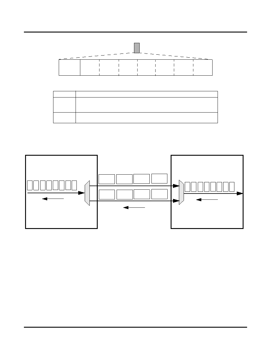
Figure 37. Link Header Byte
Table 10. Link Header Format
In cell mode, multiple SERDES links are used to achieve desired bandwidth. Data are cell-striped in a round-robin
fashion across two or eight links by the transmitter and then re-assembled back into a single cell stream (destrip-
ing) by the receiver. This is shown in Figure 38.
Figure 38. Multi-Link Interface - Two-Link Example
To assist with cell delineation, each link transmitter assigns sequence numbers to cells (LSEQN[6:0] bits in the Link
Header byte) before sending them out on the link. Each link increments its sequence numbers independently as
shown in Figure 38. All links reset their sequence number generator at the beginning of a SONET frame (All links
are synchronized to the start of a frame).
On the receiving side, each receiver uses the sequence numbers to verify the correct cell delineation. Since the
links were synchronized to the start of the SONET frame, all links will have cells with the same sequence number
available at the same time (although deskew needs to happen to properly align the cells). This allows the receiver
to correctly reconstruct the original cell stream.
If an unexpected sequence number is received, the receiver does not use the received value as the basis for the
next expected sequence number. Rather the old expected value is incremented by one, forming the new expected
value. An error ag is sent to the software register interface and the cell will be marked with an error. For example,
assume that the receiver expected to receive a cell with sequence number 27, but received one with sequence
number 37. The cell will be marked with an error. The receiver then expects to receive a cell with sequence number
28.
Location
Field/Description
7
Idle: Idle Cell Indicator
0: User Cell (contains valid data)
1: Idle Cell (no data in the cell payload)
6:0
LSEQ: Link Sequence Number. This value is used when aligning cells from
multiple links when doing link group multiplexing.
LIDLE
LSEQN[6:0]
LINK HEADER BYTE
Time
TRANSMITTER
Time
3
2
1
0
7
6
5
4
CELL STRIPING
0
1
LSEQ = 3
Cell = 7
LSEQ = 2
Cell = 5
LSEQ = 1
Cell = 3
LSEQ = 0
Cell = 1
Time
RECEIVER
3
2
1
0
7
6
5
4
CELL DE-STRIPING
0
1
LSEQ = 3
Cell = 6
LSEQ = 2
Cell = 4
LSEQ = 1
Cell = 2
LSEQ = 0
Cell = 0
相關(guān)PDF資料 |
PDF描述 |
|---|---|
| TPS2371PWR | IC PWR INTRFCE SW FOR POE 8TSSOP |
| PIC32MX575F512H-80V/PT | IC MCU 32BIT 512KB FLASH 64TQFP |
| PIC32MX775F256H-80V/PT | IC MCU 32BIT 256KB FLASH 64TQFP |
| VI-J4D-IW-F1 | CONVERTER MOD DC/DC 85V 100W |
| PIC24EP512GP806-I/MR | IC MCU 8BIT 512KB FLASH 64-QFN |
相關(guān)代理商/技術(shù)參數(shù) |
參數(shù)描述 |
|---|---|
| ORSO82G5-2FN680C1 | 功能描述:FPGA - 現(xiàn)場可編程門陣列 10368 LUT 372 I/O RoHS:否 制造商:Altera Corporation 系列:Cyclone V E 柵極數(shù)量: 邏輯塊數(shù)量:943 內(nèi)嵌式塊RAM - EBR:1956 kbit 輸入/輸出端數(shù)量:128 最大工作頻率:800 MHz 工作電源電壓:1.1 V 最大工作溫度:+ 70 C 安裝風(fēng)格:SMD/SMT 封裝 / 箱體:FBGA-256 |
| ORSO82G5-2FN680I | 功能描述:FPGA - 現(xiàn)場可編程門陣列 ORCA FPSC 2.7 Gb Bp ln Xcvr 643K Gt I RoHS:否 制造商:Altera Corporation 系列:Cyclone V E 柵極數(shù)量: 邏輯塊數(shù)量:943 內(nèi)嵌式塊RAM - EBR:1956 kbit 輸入/輸出端數(shù)量:128 最大工作頻率:800 MHz 工作電源電壓:1.1 V 最大工作溫度:+ 70 C 安裝風(fēng)格:SMD/SMT 封裝 / 箱體:FBGA-256 |
| ORSO82G5-2FN680I1 | 功能描述:FPGA - 現(xiàn)場可編程門陣列 10368 LUT 372 I/O RoHS:否 制造商:Altera Corporation 系列:Cyclone V E 柵極數(shù)量: 邏輯塊數(shù)量:943 內(nèi)嵌式塊RAM - EBR:1956 kbit 輸入/輸出端數(shù)量:128 最大工作頻率:800 MHz 工作電源電壓:1.1 V 最大工作溫度:+ 70 C 安裝風(fēng)格:SMD/SMT 封裝 / 箱體:FBGA-256 |
| ORSO82G5-3BM680C | 功能描述:FPGA - 現(xiàn)場可編程門陣列 10368 LUT 372 I/O RoHS:否 制造商:Altera Corporation 系列:Cyclone V E 柵極數(shù)量: 邏輯塊數(shù)量:943 內(nèi)嵌式塊RAM - EBR:1956 kbit 輸入/輸出端數(shù)量:128 最大工作頻率:800 MHz 工作電源電壓:1.1 V 最大工作溫度:+ 70 C 安裝風(fēng)格:SMD/SMT 封裝 / 箱體:FBGA-256 |
| ORSO82G5-3F680C | 功能描述:FPGA - 現(xiàn)場可編程門陣列 ORCA FPSC 2.7GBITS/s BP XCVR 643K RoHS:否 制造商:Altera Corporation 系列:Cyclone V E 柵極數(shù)量: 邏輯塊數(shù)量:943 內(nèi)嵌式塊RAM - EBR:1956 kbit 輸入/輸出端數(shù)量:128 最大工作頻率:800 MHz 工作電源電壓:1.1 V 最大工作溫度:+ 70 C 安裝風(fēng)格:SMD/SMT 封裝 / 箱體:FBGA-256 |
發(fā)布緊急采購,3分鐘左右您將得到回復(fù)。