- 您現(xiàn)在的位置:買賣IC網(wǎng) > PDF目錄11733 > ORSO82G5-2FN680C (Lattice Semiconductor Corporation)IC TRANCEIVERS FPSC 680FPBGA PDF資料下載
參數(shù)資料
| 型號(hào): | ORSO82G5-2FN680C |
| 廠商: | Lattice Semiconductor Corporation |
| 文件頁(yè)數(shù): | 76/153頁(yè) |
| 文件大小: | 0K |
| 描述: | IC TRANCEIVERS FPSC 680FPBGA |
| 產(chǎn)品變化通告: | Product Discontinuation 01/Aug/2011 |
| 標(biāo)準(zhǔn)包裝: | 24 |
| 系列: | * |
第1頁(yè)第2頁(yè)第3頁(yè)第4頁(yè)第5頁(yè)第6頁(yè)第7頁(yè)第8頁(yè)第9頁(yè)第10頁(yè)第11頁(yè)第12頁(yè)第13頁(yè)第14頁(yè)第15頁(yè)第16頁(yè)第17頁(yè)第18頁(yè)第19頁(yè)第20頁(yè)第21頁(yè)第22頁(yè)第23頁(yè)第24頁(yè)第25頁(yè)第26頁(yè)第27頁(yè)第28頁(yè)第29頁(yè)第30頁(yè)第31頁(yè)第32頁(yè)第33頁(yè)第34頁(yè)第35頁(yè)第36頁(yè)第37頁(yè)第38頁(yè)第39頁(yè)第40頁(yè)第41頁(yè)第42頁(yè)第43頁(yè)第44頁(yè)第45頁(yè)第46頁(yè)第47頁(yè)第48頁(yè)第49頁(yè)第50頁(yè)第51頁(yè)第52頁(yè)第53頁(yè)第54頁(yè)第55頁(yè)第56頁(yè)第57頁(yè)第58頁(yè)第59頁(yè)第60頁(yè)第61頁(yè)第62頁(yè)第63頁(yè)第64頁(yè)第65頁(yè)第66頁(yè)第67頁(yè)第68頁(yè)第69頁(yè)第70頁(yè)第71頁(yè)第72頁(yè)第73頁(yè)第74頁(yè)第75頁(yè)當(dāng)前第76頁(yè)第77頁(yè)第78頁(yè)第79頁(yè)第80頁(yè)第81頁(yè)第82頁(yè)第83頁(yè)第84頁(yè)第85頁(yè)第86頁(yè)第87頁(yè)第88頁(yè)第89頁(yè)第90頁(yè)第91頁(yè)第92頁(yè)第93頁(yè)第94頁(yè)第95頁(yè)第96頁(yè)第97頁(yè)第98頁(yè)第99頁(yè)第100頁(yè)第101頁(yè)第102頁(yè)第103頁(yè)第104頁(yè)第105頁(yè)第106頁(yè)第107頁(yè)第108頁(yè)第109頁(yè)第110頁(yè)第111頁(yè)第112頁(yè)第113頁(yè)第114頁(yè)第115頁(yè)第116頁(yè)第117頁(yè)第118頁(yè)第119頁(yè)第120頁(yè)第121頁(yè)第122頁(yè)第123頁(yè)第124頁(yè)第125頁(yè)第126頁(yè)第127頁(yè)第128頁(yè)第129頁(yè)第130頁(yè)第131頁(yè)第132頁(yè)第133頁(yè)第134頁(yè)第135頁(yè)第136頁(yè)第137頁(yè)第138頁(yè)第139頁(yè)第140頁(yè)第141頁(yè)第142頁(yè)第143頁(yè)第144頁(yè)第145頁(yè)第146頁(yè)第147頁(yè)第148頁(yè)第149頁(yè)第150頁(yè)第151頁(yè)第152頁(yè)第153頁(yè)
Lattice Semiconductor
ORCA ORSO42G5 and ORSO82G5 Data Sheet
29
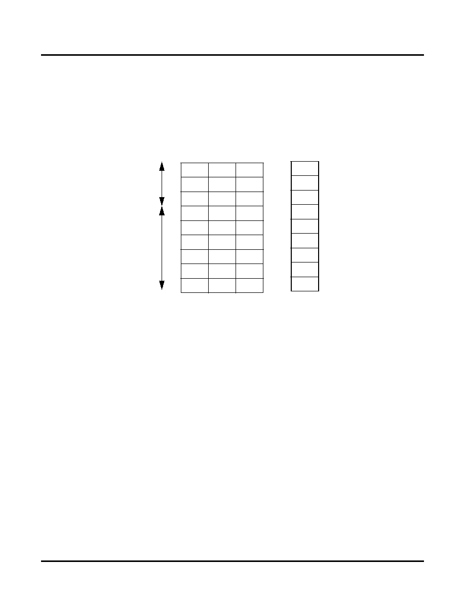
SONET TOH Byte Denitions
The Transport OverHead bytes of the SONET frame can be used for in-band conguration, service, and manage-
ment since it is carried along the same channel as data. In the ORSO42G5 and ORSO82G5 in-band signaling can
be efciently utilized, since the total cost of overhead is only 3.3%. The overhead bytes in an STS-1 header are
shown in Table 15 (The path overhead bytes are in the SPE.)
Figure 15. SONET Overhead Bytes
When used in true SONET applications, all or most TOH bytes will be generated in the FPGA logic or by an exter-
nal device. Two modes are provided for this application – transparent and AUTO_SOH. In transparent mode all
bytes from the FPGA logic are passed through unchanged.
In AUTO_SOH mode the embedded core inserts the A1/A2 framing bytes, performs the B1 calculation and inserts
the B1 byte. A1/A2 and B1 insertion can be independently enabled. This avoids the need to do SONET scrambling
in the FPGA logic. All other bytes are passed through unchanged from the FPGA logic as in transparent mode.
When used for applications that transfer non-SONET data, an AUTO_TOH mode is provided. In this mode, all of
the overhead bytes are set by the embedded core. Most of the bytes are set to zero. At the receive side, all of the
TOH bytes except those set to a non-zero value can be ignored in the AUTO_TOH mode.
The TOH bytes have the following functions in true SONET applications.
Section Overhead Bytes:
– A1, A2 – These bytes are used for framing and to mark the beginning of a SONET frame. A1 has the value
0x F6 and A2 has the value 0x28.
– J0 -Section Trace Message – This byte carries the section trace message. The message is interpreted to
verify connectivity to a particular node in the network.
– B1 - Section Bit Interleaved Parity (BIP-8) byte – This byte carries the parity information which is used to
check for transmission errors in a section. The computed parity value is transmitted in the next frame in the
B1 position. It is dened only for the rst STS-1 of a STS-N signal. The other bytes have a default value of
0x00.
J1
B3
C2
H4
G1
F2
Z4
Z5
Z6
A1
A2
J0
B1
E1
F1
D1
D2
D3
H1
H2
H3
B2
K1
K2
D4
D5
D6
D7
D8
D9
D10
D11
D12
S1/Z1
Z3
E2
J1
B3
C2
H4
G1
F2
Z4
Z5
Z6
0
1
4
3
2
5
6
7
8
Transport
Overhead
Path
Overhead
012
Line
Overhead
Section
Overhead
相關(guān)PDF資料 |
PDF描述 |
|---|---|
| TPS2371PWR | IC PWR INTRFCE SW FOR POE 8TSSOP |
| PIC32MX575F512H-80V/PT | IC MCU 32BIT 512KB FLASH 64TQFP |
| PIC32MX775F256H-80V/PT | IC MCU 32BIT 256KB FLASH 64TQFP |
| VI-J4D-IW-F1 | CONVERTER MOD DC/DC 85V 100W |
| PIC24EP512GP806-I/MR | IC MCU 8BIT 512KB FLASH 64-QFN |
相關(guān)代理商/技術(shù)參數(shù) |
參數(shù)描述 |
|---|---|
| ORSO82G5-2FN680C1 | 功能描述:FPGA - 現(xiàn)場(chǎng)可編程門陣列 10368 LUT 372 I/O RoHS:否 制造商:Altera Corporation 系列:Cyclone V E 柵極數(shù)量: 邏輯塊數(shù)量:943 內(nèi)嵌式塊RAM - EBR:1956 kbit 輸入/輸出端數(shù)量:128 最大工作頻率:800 MHz 工作電源電壓:1.1 V 最大工作溫度:+ 70 C 安裝風(fēng)格:SMD/SMT 封裝 / 箱體:FBGA-256 |
| ORSO82G5-2FN680I | 功能描述:FPGA - 現(xiàn)場(chǎng)可編程門陣列 ORCA FPSC 2.7 Gb Bp ln Xcvr 643K Gt I RoHS:否 制造商:Altera Corporation 系列:Cyclone V E 柵極數(shù)量: 邏輯塊數(shù)量:943 內(nèi)嵌式塊RAM - EBR:1956 kbit 輸入/輸出端數(shù)量:128 最大工作頻率:800 MHz 工作電源電壓:1.1 V 最大工作溫度:+ 70 C 安裝風(fēng)格:SMD/SMT 封裝 / 箱體:FBGA-256 |
| ORSO82G5-2FN680I1 | 功能描述:FPGA - 現(xiàn)場(chǎng)可編程門陣列 10368 LUT 372 I/O RoHS:否 制造商:Altera Corporation 系列:Cyclone V E 柵極數(shù)量: 邏輯塊數(shù)量:943 內(nèi)嵌式塊RAM - EBR:1956 kbit 輸入/輸出端數(shù)量:128 最大工作頻率:800 MHz 工作電源電壓:1.1 V 最大工作溫度:+ 70 C 安裝風(fēng)格:SMD/SMT 封裝 / 箱體:FBGA-256 |
| ORSO82G5-3BM680C | 功能描述:FPGA - 現(xiàn)場(chǎng)可編程門陣列 10368 LUT 372 I/O RoHS:否 制造商:Altera Corporation 系列:Cyclone V E 柵極數(shù)量: 邏輯塊數(shù)量:943 內(nèi)嵌式塊RAM - EBR:1956 kbit 輸入/輸出端數(shù)量:128 最大工作頻率:800 MHz 工作電源電壓:1.1 V 最大工作溫度:+ 70 C 安裝風(fēng)格:SMD/SMT 封裝 / 箱體:FBGA-256 |
| ORSO82G5-3F680C | 功能描述:FPGA - 現(xiàn)場(chǎng)可編程門陣列 ORCA FPSC 2.7GBITS/s BP XCVR 643K RoHS:否 制造商:Altera Corporation 系列:Cyclone V E 柵極數(shù)量: 邏輯塊數(shù)量:943 內(nèi)嵌式塊RAM - EBR:1956 kbit 輸入/輸出端數(shù)量:128 最大工作頻率:800 MHz 工作電源電壓:1.1 V 最大工作溫度:+ 70 C 安裝風(fēng)格:SMD/SMT 封裝 / 箱體:FBGA-256 |
發(fā)布緊急采購(gòu),3分鐘左右您將得到回復(fù)。