- 您現(xiàn)在的位置:買賣IC網(wǎng) > PDF目錄11733 > ORSO82G5-3FN680C (Lattice Semiconductor Corporation)IC TRANCEIVERS FPSC 680FPBGA PDF資料下載
參數(shù)資料
| 型號(hào): | ORSO82G5-3FN680C |
| 廠商: | Lattice Semiconductor Corporation |
| 文件頁數(shù): | 63/153頁 |
| 文件大小: | 0K |
| 描述: | IC TRANCEIVERS FPSC 680FPBGA |
| 產(chǎn)品變化通告: | Product Discontinuation 01/Aug/2011 |
| 標(biāo)準(zhǔn)包裝: | 24 |
| 系列: | * |
第1頁第2頁第3頁第4頁第5頁第6頁第7頁第8頁第9頁第10頁第11頁第12頁第13頁第14頁第15頁第16頁第17頁第18頁第19頁第20頁第21頁第22頁第23頁第24頁第25頁第26頁第27頁第28頁第29頁第30頁第31頁第32頁第33頁第34頁第35頁第36頁第37頁第38頁第39頁第40頁第41頁第42頁第43頁第44頁第45頁第46頁第47頁第48頁第49頁第50頁第51頁第52頁第53頁第54頁第55頁第56頁第57頁第58頁第59頁第60頁第61頁第62頁當(dāng)前第63頁第64頁第65頁第66頁第67頁第68頁第69頁第70頁第71頁第72頁第73頁第74頁第75頁第76頁第77頁第78頁第79頁第80頁第81頁第82頁第83頁第84頁第85頁第86頁第87頁第88頁第89頁第90頁第91頁第92頁第93頁第94頁第95頁第96頁第97頁第98頁第99頁第100頁第101頁第102頁第103頁第104頁第105頁第106頁第107頁第108頁第109頁第110頁第111頁第112頁第113頁第114頁第115頁第116頁第117頁第118頁第119頁第120頁第121頁第122頁第123頁第124頁第125頁第126頁第127頁第128頁第129頁第130頁第131頁第132頁第133頁第134頁第135頁第136頁第137頁第138頁第139頁第140頁第141頁第142頁第143頁第144頁第145頁第146頁第147頁第148頁第149頁第150頁第151頁第152頁第153頁
Lattice Semiconductor
ORCA ORSO42G5 and ORSO82G5 Data Sheet
17
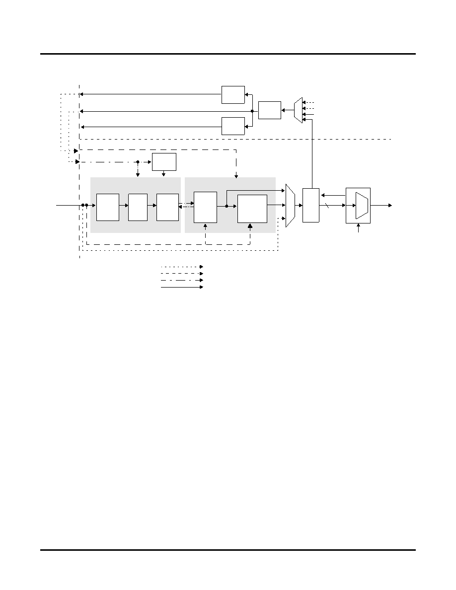
Figure 3. Top Level Overview, TX Path Logic, Single Channel
Receiver Architecture
The receiver section receives high-speed serial data at the external differential CML input pins. These data are fed
to the clock recovery section which generates a recovered clock and retimes the data. Therefore the receive clocks
are asynchronous between channels. The data are then optionally framed, reformatted, aligned and passed to the
FPGA logic in various parallel data formats.
The top level receiver architecture is shown in Figure 4. The main logical blocks in the receive path are:
Receive SERDES and 8:32 DEMUX.
SONET processing logic.
Input Port Controllers (IPCs) which contain the cell processing logic.
Depending on the mode of operation, the FPGA to backplane data path may include or bypass the various logical
blocks.
FPGA Logic
Embedded Core
SONET
Scrambler
TOH
Block
TX
FIFO
32:8
MUX
OPC2/
OPC8
Payload
Block
Cell Processing
SONET Processing
600 Mb/s
- 2.7 Gb/s
SERDES
8
LDIN
xck311
1:8
Demux
Legend:
TCK39x
TCK78x
TCK156x
TSYSCLKx[A:D]
x = A for Block A, B for Block B
SYSCLK 156 8 (*ORSO82G5 only)
Line Key:
311MHz from
Other Links
in Block
77.76 MHz
SYSCLK156x[1:2]
TSYSCLKx[A:D]
TCK39x
TCK156x
TCK78X
REFCLK (155.52MHz)
nominal
Logic Common to Block
311MHz
SERDES-Only Mode
SONET Mode
Cell Mode
Cell/SONET or All Modes
Data
from
FPGA
or SYSCLK156 8*
Divide
by 2
Divide
by 2
Divide
by 2
Divide
by 4
SONET
Scrambler
相關(guān)PDF資料 |
PDF描述 |
|---|---|
| PIC32MX675F256L-80I/PT | IC MCU 32BIT 256KB FLASH 100TQFP |
| D38999/26FE26SC | CONN PLUG 26POS STRAIGHT W/SCKT |
| MSP430F4783IPZ | IC MCU 16BIT 48KB FLASH 100LQFP |
| MS27656T17F99S | CONN RCPT 23POS WALL MNT W/SCKT |
| VI-J4B-IW-F3 | CONVERTER MOD DC/DC 95V 100W |
相關(guān)代理商/技術(shù)參數(shù) |
參數(shù)描述 |
|---|---|
| ORSO82G5-3FN680C1 | 功能描述:FPGA - 現(xiàn)場可編程門陣列 10368 LUT 372 I/O RoHS:否 制造商:Altera Corporation 系列:Cyclone V E 柵極數(shù)量: 邏輯塊數(shù)量:943 內(nèi)嵌式塊RAM - EBR:1956 kbit 輸入/輸出端數(shù)量:128 最大工作頻率:800 MHz 工作電源電壓:1.1 V 最大工作溫度:+ 70 C 安裝風(fēng)格:SMD/SMT 封裝 / 箱體:FBGA-256 |
| ORSO82G5-G2-PAC-EV | 功能描述:可編程邏輯 IC 開發(fā)工具 ORCA ORSO82G5-FPSC Eval Brd RoHS:否 制造商:Altera Corporation 產(chǎn)品:Development Kits 類型:FPGA 工具用于評(píng)估:5CEFA7F3 接口類型: 工作電源電壓: |
| ORSPI4 | 制造商:LATTICE 制造商全稱:Lattice Semiconductor 功能描述:Dual SPI4 Interface and High-Speed SERDES FPSC |
| ORSPI4-1F1156C | 功能描述:FPGA - 現(xiàn)場可編程門陣列 16192 LUT RoHS:否 制造商:Altera Corporation 系列:Cyclone V E 柵極數(shù)量: 邏輯塊數(shù)量:943 內(nèi)嵌式塊RAM - EBR:1956 kbit 輸入/輸出端數(shù)量:128 最大工作頻率:800 MHz 工作電源電壓:1.1 V 最大工作溫度:+ 70 C 安裝風(fēng)格:SMD/SMT 封裝 / 箱體:FBGA-256 |
| ORSPI4-1F1156I | 功能描述:FPGA - 現(xiàn)場可編程門陣列 16192 LUT RoHS:否 制造商:Altera Corporation 系列:Cyclone V E 柵極數(shù)量: 邏輯塊數(shù)量:943 內(nèi)嵌式塊RAM - EBR:1956 kbit 輸入/輸出端數(shù)量:128 最大工作頻率:800 MHz 工作電源電壓:1.1 V 最大工作溫度:+ 70 C 安裝風(fēng)格:SMD/SMT 封裝 / 箱體:FBGA-256 |
發(fā)布緊急采購,3分鐘左右您將得到回復(fù)。