- 您現(xiàn)在的位置:買(mǎi)賣(mài)IC網(wǎng) > PDF目錄11733 > ORT82G5-2FN680C (Lattice Semiconductor Corporation)IC TRANCEIVERS FPSC 680FPBGA PDF資料下載
參數(shù)資料
| 型號(hào): | ORT82G5-2FN680C |
| 廠商: | Lattice Semiconductor Corporation |
| 文件頁(yè)數(shù): | 95/119頁(yè) |
| 文件大小: | 0K |
| 描述: | IC TRANCEIVERS FPSC 680FPBGA |
| 產(chǎn)品變化通告: | Product Discontinuation 01/Aug/2011 |
| 標(biāo)準(zhǔn)包裝: | 24 |
| 系列: | * |
第1頁(yè)第2頁(yè)第3頁(yè)第4頁(yè)第5頁(yè)第6頁(yè)第7頁(yè)第8頁(yè)第9頁(yè)第10頁(yè)第11頁(yè)第12頁(yè)第13頁(yè)第14頁(yè)第15頁(yè)第16頁(yè)第17頁(yè)第18頁(yè)第19頁(yè)第20頁(yè)第21頁(yè)第22頁(yè)第23頁(yè)第24頁(yè)第25頁(yè)第26頁(yè)第27頁(yè)第28頁(yè)第29頁(yè)第30頁(yè)第31頁(yè)第32頁(yè)第33頁(yè)第34頁(yè)第35頁(yè)第36頁(yè)第37頁(yè)第38頁(yè)第39頁(yè)第40頁(yè)第41頁(yè)第42頁(yè)第43頁(yè)第44頁(yè)第45頁(yè)第46頁(yè)第47頁(yè)第48頁(yè)第49頁(yè)第50頁(yè)第51頁(yè)第52頁(yè)第53頁(yè)第54頁(yè)第55頁(yè)第56頁(yè)第57頁(yè)第58頁(yè)第59頁(yè)第60頁(yè)第61頁(yè)第62頁(yè)第63頁(yè)第64頁(yè)第65頁(yè)第66頁(yè)第67頁(yè)第68頁(yè)第69頁(yè)第70頁(yè)第71頁(yè)第72頁(yè)第73頁(yè)第74頁(yè)第75頁(yè)第76頁(yè)第77頁(yè)第78頁(yè)第79頁(yè)第80頁(yè)第81頁(yè)第82頁(yè)第83頁(yè)第84頁(yè)第85頁(yè)第86頁(yè)第87頁(yè)第88頁(yè)第89頁(yè)第90頁(yè)第91頁(yè)第92頁(yè)第93頁(yè)第94頁(yè)當(dāng)前第95頁(yè)第96頁(yè)第97頁(yè)第98頁(yè)第99頁(yè)第100頁(yè)第101頁(yè)第102頁(yè)第103頁(yè)第104頁(yè)第105頁(yè)第106頁(yè)第107頁(yè)第108頁(yè)第109頁(yè)第110頁(yè)第111頁(yè)第112頁(yè)第113頁(yè)第114頁(yè)第115頁(yè)第116頁(yè)第117頁(yè)第118頁(yè)第119頁(yè)
Lattice Semiconductor
ORCA ORT42G5 and ORT82G5 Data Sheet
77
High Speed Data Receiver
Table 35 species receiver parameters measured on devices with worst case process parameters and over the full
range of operation conditions.
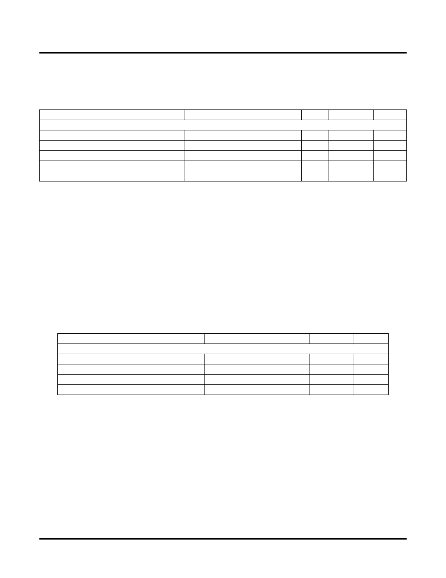
Table 35. External Data Input Specications
Input Data Jitter Tolerance
A receiver’s ability to tolerate incoming signal jitter is very dependent on jitter type. High speed serial interface stan-
dards have recognized the dependency on jitter type and have recently modified specifications to indicate toler-
ance levels for different jitter types as they relate to specific protocols (e.g XAUI, FC, Infiniband etc.). Sinusoidal
jitter is considered to be a worst case jitter type. Table 36 shows receiver specifications with 10 MHz sinusoidal jit-
ter injection. XAUI specic jitter tolerance measurements were measured in a separate experiment detailed in tech-
nical note TN1032, SERDES Test Chip Jitter, and are not reected in these results.
Table 36. Receiver Sinusoidal Jitter Tolerance Specications
Parameter
Conditions
Min.
Typ.
Max.
Units
Input Data
Stream of Nontransitions
8b/10b encode/decode off
—
72
Bits
Sensitivity (differential), worst-case
1
3.125 Gbps
80
—
mVp-p
Input Levels
2
—
VSS - 0.3
—
VDD_ANA + 0.3
V
Internal Buffer Resistance (Each input to VDDIB)
—
40
50
60
Ω
PLL Lock Time
3
—
Note 2
—
1. With PRBS 2^7-1 data pattern, all channels operating, FPGA logic active, REFCLK jitter of 30 ps., TA = 0
oC to 85oC, 1.425V to 1.575V sup-
ply.
2. Input level min + (input peak to peak swing)/2 ≤ common mode input voltage ≤ input level max - (input peak to peak swing)/2
3. The ORT42G5 and ORT82G5 SERDES receiver performs four levels of synchronization on the incoming serial data stream, providing rst
bit, then byte (character), then channel (32-bit word), and nally optional multi-channel alignment as described in TN1025. The PLL Lock
Time is the time required for the CDR PLL to lock to the transitions in the incoming high-speed serial data stream. If the PLL is unable to
lock to the serial data stream, it instead locks to REFCLK to stabilize the voltage-controlled oscillator (VCO), and periodically switches back
to the serial data stream to again attempt synchronization.
Parameter
Conditions
Max.
Unit
Input Data
Jitter Tolerance @3.125Gbps, Typical
600 mV diff eye
1
0.75
UIP-P
Jitter Tolerance @3.125Gbps, Worst case
600 mV diff eye
1
0.65
UIP-P
Jitter Tolerance @2.5Gbps,Typical
600 mV diff eye
1
0.79
UIP-P
Jitter Tolerance @2.5Gbps, Worst case
600 mV diff eye
1
0.67
UIP-P
1. With PRBS 2^7-1 data pattern, all channels operating, FPGA logic active, REFCLK jitter of 30 ps., TA = 0
oC to 85oC, 1.425V
to 1.575V supply. Jitter measured with a Wavecrest SIA-3000.
相關(guān)PDF資料 |
PDF描述 |
|---|---|
| MSP430F4793IPZ | IC MCU 16BIT 60KB FLASH 100LQFP |
| VE-J4B-IW-F3 | CONVERTER MOD DC/DC 95V 100W |
| PIC18F4510-I/ML | IC MCU FLASH 16KX16 44QFN |
| VE-J4B-IW-F2 | CONVERTER MOD DC/DC 95V 100W |
| PIC32MX675F256L-80I/PF | IC MCU 32BIT 256KB FLASH 100TQFP |
相關(guān)代理商/技術(shù)參數(shù) |
參數(shù)描述 |
|---|---|
| ORT82G5-2FN680C1 | 功能描述:FPGA - 現(xiàn)場(chǎng)可編程門(mén)陣列 10368 LUT 372 I/O RoHS:否 制造商:Altera Corporation 系列:Cyclone V E 柵極數(shù)量: 邏輯塊數(shù)量:943 內(nèi)嵌式塊RAM - EBR:1956 kbit 輸入/輸出端數(shù)量:128 最大工作頻率:800 MHz 工作電源電壓:1.1 V 最大工作溫度:+ 70 C 安裝風(fēng)格:SMD/SMT 封裝 / 箱體:FBGA-256 |
| ORT82G5-2FN680I | 功能描述:FPGA - 現(xiàn)場(chǎng)可編程門(mén)陣列 ORCA FPSC 3.7 Gb Bp ln Xcvr 643K Gt I RoHS:否 制造商:Altera Corporation 系列:Cyclone V E 柵極數(shù)量: 邏輯塊數(shù)量:943 內(nèi)嵌式塊RAM - EBR:1956 kbit 輸入/輸出端數(shù)量:128 最大工作頻率:800 MHz 工作電源電壓:1.1 V 最大工作溫度:+ 70 C 安裝風(fēng)格:SMD/SMT 封裝 / 箱體:FBGA-256 |
| ORT82G5-2FN680I1 | 功能描述:FPGA - 現(xiàn)場(chǎng)可編程門(mén)陣列 10368 LUT 372 I/O RoHS:否 制造商:Altera Corporation 系列:Cyclone V E 柵極數(shù)量: 邏輯塊數(shù)量:943 內(nèi)嵌式塊RAM - EBR:1956 kbit 輸入/輸出端數(shù)量:128 最大工作頻率:800 MHz 工作電源電壓:1.1 V 最大工作溫度:+ 70 C 安裝風(fēng)格:SMD/SMT 封裝 / 箱體:FBGA-256 |
| ORT82G5-3BM680C | 功能描述:FPGA - 現(xiàn)場(chǎng)可編程門(mén)陣列 10368 LUT 372 I/O RoHS:否 制造商:Altera Corporation 系列:Cyclone V E 柵極數(shù)量: 邏輯塊數(shù)量:943 內(nèi)嵌式塊RAM - EBR:1956 kbit 輸入/輸出端數(shù)量:128 最大工作頻率:800 MHz 工作電源電壓:1.1 V 最大工作溫度:+ 70 C 安裝風(fēng)格:SMD/SMT 封裝 / 箱體:FBGA-256 |
| ORT82G5-3BM680C2 | 制造商:LATTICE 制造商全稱:Lattice Semiconductor 功能描述:0.6 to 3.7 Gbps XAUI and FC FPSCs |
發(fā)布緊急采購(gòu),3分鐘左右您將得到回復(fù)。