- 您現(xiàn)在的位置:買賣IC網(wǎng) > PDF目錄378055 > PM5945-UTP5 (PMC-Sierra, Inc.) ATM PHYSICAL INTERFACE APPLICATION BOARD FOR CAT-5 UTP PDF資料下載
參數(shù)資料
| 型號(hào): | PM5945-UTP5 |
| 廠商: | PMC-Sierra, Inc. |
| 英文描述: | ATM PHYSICAL INTERFACE APPLICATION BOARD FOR CAT-5 UTP |
| 中文描述: | ATM物理接口貓應(yīng)用板- 5雙絞線 |
| 文件頁(yè)數(shù): | 17/84頁(yè) |
| 文件大小: | 1666K |
| 代理商: | PM5945-UTP5 |
第1頁(yè)第2頁(yè)第3頁(yè)第4頁(yè)第5頁(yè)第6頁(yè)第7頁(yè)第8頁(yè)第9頁(yè)第10頁(yè)第11頁(yè)第12頁(yè)第13頁(yè)第14頁(yè)第15頁(yè)第16頁(yè)當(dāng)前第17頁(yè)第18頁(yè)第19頁(yè)第20頁(yè)第21頁(yè)第22頁(yè)第23頁(yè)第24頁(yè)第25頁(yè)第26頁(yè)第27頁(yè)第28頁(yè)第29頁(yè)第30頁(yè)第31頁(yè)第32頁(yè)第33頁(yè)第34頁(yè)第35頁(yè)第36頁(yè)第37頁(yè)第38頁(yè)第39頁(yè)第40頁(yè)第41頁(yè)第42頁(yè)第43頁(yè)第44頁(yè)第45頁(yè)第46頁(yè)第47頁(yè)第48頁(yè)第49頁(yè)第50頁(yè)第51頁(yè)第52頁(yè)第53頁(yè)第54頁(yè)第55頁(yè)第56頁(yè)第57頁(yè)第58頁(yè)第59頁(yè)第60頁(yè)第61頁(yè)第62頁(yè)第63頁(yè)第64頁(yè)第65頁(yè)第66頁(yè)第67頁(yè)第68頁(yè)第69頁(yè)第70頁(yè)第71頁(yè)第72頁(yè)第73頁(yè)第74頁(yè)第75頁(yè)第76頁(yè)第77頁(yè)第78頁(yè)第79頁(yè)第80頁(yè)第81頁(yè)第82頁(yè)第83頁(yè)第84頁(yè)
S
TANDARD
P
RODUCT
PMC-Sierra, Inc.
PM5945 -UTP5
PMC-940202 ISSUE 2. APRIL 7, 1995
______________________________________________________________________________________________
APP_SAPI_UTP5
______________________________________________________________________________________________
13
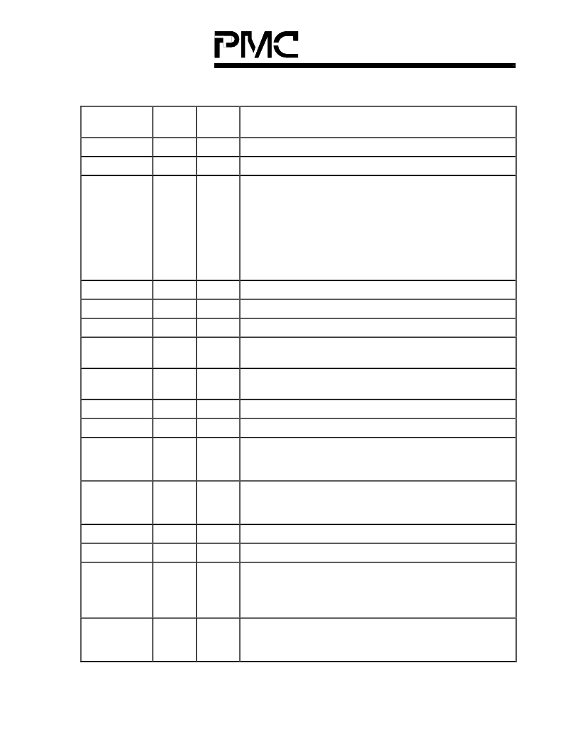
Signal
Name
GND
GND
TxDat[0]
TxDat[1]
TxDat[2]
TxDat[3]
TxDat[4]
TxDat[5]
TxDat[6]
TxDat[7]
VCC
VCC
GND
TxPrty
Type
Power
Power
I
I
I
I
I
I
I
I
Power
Power
Power
I
PIN
1
2
3
5
9
11
4
6
10
12
Function
Ground
Ground
The S/UNI is configured for the 8 bit FIFO interface,
TxDat[7:0] corresponds to a cell byte.
TxDat[7] corresponds to bit 1, the first bit received.
TxDat[0] corresponds to bit 8, the last bit received.
7
8
13
14
+5 Volts
+5 Volts
Ground
Transmit data bus (TxDat[7:0]) odd parity. Not
Used
Transmit start of cell indication. Identifies the first
byte (word) of a cell on inputs TxDAT[7:0]
Ground
Ground
Active low signal from the PHY to ATM layer,
asserted by the PHY layer 4 cycles before it is no
longer able to accept transmit data.
Active low signal from the ATM layer to the PHY
layer, asserted by the ATM layer when it has a full
cell to transmit.
Ground
Ground
The transmit transfer/synchronization clock
provided by the ATM to the PHY layer for
synchronizing transfers on the TxDATA bus.
(nominally at 20 MHz).
Transmit Reference. Input for the purposes of
synchronization (e.g. 8 KHz frame marker or
SONET frame indicator). Not Used
TxSOC
I
15
GND
GND
TxFullB
Power
Power
O
16
17
18
TxClavB
I
19
GND
GND
TxCLK
Power
Power
I
20
21
22
TxRefB
I
23
相關(guān)PDF資料 |
PDF描述 |
|---|---|
| PM5945 | CONN |
| PM6341 | E1 TRANSCEIVER |
| PM6341-QI | Ultraframer DS3/E3/DS2/E2/DS1/E1/DS0 |
| PM6341-RI | Ultraframer DS3/E3/DS2/E2/DS1/E1/DS0 |
| PM6344-RI | KPSE SERIES |
相關(guān)代理商/技術(shù)參數(shù) |
參數(shù)描述 |
|---|---|
| PM594D | 制造商:未知廠家 制造商全稱:未知廠家 功能描述:Analog IC |
| PM594DS | 制造商:未知廠家 制造商全稱:未知廠家 功能描述:Analog IC |
| PM594K | 制造商:未知廠家 制造商全稱:未知廠家 功能描述:Analog IC |
| PM594KS | 制造商:未知廠家 制造商全稱:未知廠家 功能描述:Analog IC |
| PM594S | 制造商:未知廠家 制造商全稱:未知廠家 功能描述:Analog IC |
發(fā)布緊急采購(gòu),3分鐘左右您將得到回復(fù)。