- 您現(xiàn)在的位置:買賣IC網(wǎng) > PDF目錄296936 > QL1P100-8PUN86M (QUICKLOGIC CORP) FPGA, 640 CLBS, 100000 GATES, PBGA86 PDF資料下載
參數(shù)資料
| 型號: | QL1P100-8PUN86M |
| 廠商: | QUICKLOGIC CORP |
| 元件分類: | FPGA |
| 英文描述: | FPGA, 640 CLBS, 100000 GATES, PBGA86 |
| 封裝: | 6 X 6 MM, 1.20 MM HEIGHT, 0.50 MM PITCH, LEAD FREE, TFBGA-86 |
| 文件頁數(shù): | 11/44頁 |
| 文件大?。?/td> | 1101K |
| 代理商: | QL1P100-8PUN86M |
第1頁第2頁第3頁第4頁第5頁第6頁第7頁第8頁第9頁第10頁當(dāng)前第11頁第12頁第13頁第14頁第15頁第16頁第17頁第18頁第19頁第20頁第21頁第22頁第23頁第24頁第25頁第26頁第27頁第28頁第29頁第30頁第31頁第32頁第33頁第34頁第35頁第36頁第37頁第38頁第39頁第40頁第41頁第42頁第43頁第44頁
2010 QuickLogic Corporation
QuickLogic PolarPro Device Data Sheet — 86-Pin TFBGA QL1P100 Rev. G
19
Very Low Power (VLP) Mode
The QuickLogic PolarPro devices have a unique feature, referred to as VLP mode, which reduces power
consumption by placing the device in standby. Specifically, VLP mode can bring the total standby current down
to less than 10 A at room temperature when no incoming signals are toggled. VLP mode is controlled by the
VLP pin. The VLP pin is active low, so VLP mode is activated by pulling the VLP pin to ground. Conversely,
the VLP pin must be pulled to 3.3 V for normal operation.
When a PolarPro device goes into VLP mode, the following occurs:
All logic cell registers and GPIO registers values are held
All RAM cell data is retained
The outputs from all GPIO to the internal logic are tied to a weak ‘1’
GPIO outputs drive the previous values
GPIO output enables retain the previous values
DDRIO outputs are pulled down through a weak pull down circuit
Clock pad inputs are gated
CCMs are held in the reset state
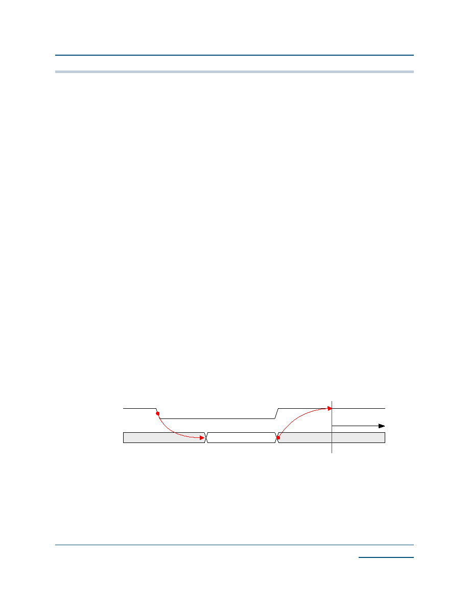
The entire operation from normal mode to VLP mode requires 250 s (300 s maximum). As mentioned in
the VLP behavioral description above, the output of the GPIO to the internal logic is a weak ‘1’. Therefore,
to preserve data retention GPIO should not be used for a set, reset, or clock signal. During the transition from
VLP mode to normal operation, the VLP pin can draw up to 1.5 mA. Consequently, if using a pull-up resistor,
use a pull-up resistor with a value that is less than 2 K
.
As the device exits out of VLP mode, the data from the registers, RAM, and GPIO will be used to recover the
functionality of the device. Furthermore, since the CCMs were in a reset state during VLP mode, they will have
to re-acquire the correct output signals before asserting lock_out. The time required to go from VLP mode to
normal operation is 250 s (300 s maximum). Figure 14 displays the delays associated with entering and
exiting VLP mode.
Figure 14: Typical VLP Mode Timing
VLP pin
VLP status
VLP mode
Normal
Operation
VLP inactive
250us
相關(guān)PDF資料 |
PDF描述 |
|---|---|
| QL2003-2PF144I | Field Programmable Gate Array (FPGA) |
| QL2003-2PL84C | Field Programmable Gate Array (FPGA) |
| QL2003-2PL84I | Field Programmable Gate Array (FPGA) |
| QL2003-XPF100C | Field Programmable Gate Array (FPGA) |
| QL2003-XPF100I | Field Programmable Gate Array (FPGA) |
相關(guān)代理商/技術(shù)參數(shù) |
參數(shù)描述 |
|---|---|
| QL-1RED | 制造商:Panduit Corp 功能描述: |
| QL-1WHT | 制造商:Panduit Corp 功能描述: |
| QL-1YEL | 制造商:Panduit Corp 功能描述:B-SI |
| QL2003 | 制造商:未知廠家 制造商全稱:未知廠家 功能描述:3.3V and 5.0V pASIC-R 2 FPGA Combining Speed, Density, Low Cost and Flexibility |
| QL2003-0PF100C | 制造商:未知廠家 制造商全稱:未知廠家 功能描述:Field Programmable Gate Array (FPGA) |
發(fā)布緊急采購,3分鐘左右您將得到回復(fù)。