- 您現(xiàn)在的位置:買賣IC網(wǎng) > PDF目錄373273 > RH80532NC017256 Microprocessor PDF資料下載
參數(shù)資料
| 型號(hào): | RH80532NC017256 |
| 元件分類: | 微處理器 |
| 英文描述: | Microprocessor |
| 中文描述: | 微處理器 |
| 文件頁(yè)數(shù): | 39/93頁(yè) |
| 文件大小: | 2353K |
| 代理商: | RH80532NC017256 |
第1頁(yè)第2頁(yè)第3頁(yè)第4頁(yè)第5頁(yè)第6頁(yè)第7頁(yè)第8頁(yè)第9頁(yè)第10頁(yè)第11頁(yè)第12頁(yè)第13頁(yè)第14頁(yè)第15頁(yè)第16頁(yè)第17頁(yè)第18頁(yè)第19頁(yè)第20頁(yè)第21頁(yè)第22頁(yè)第23頁(yè)第24頁(yè)第25頁(yè)第26頁(yè)第27頁(yè)第28頁(yè)第29頁(yè)第30頁(yè)第31頁(yè)第32頁(yè)第33頁(yè)第34頁(yè)第35頁(yè)第36頁(yè)第37頁(yè)第38頁(yè)當(dāng)前第39頁(yè)第40頁(yè)第41頁(yè)第42頁(yè)第43頁(yè)第44頁(yè)第45頁(yè)第46頁(yè)第47頁(yè)第48頁(yè)第49頁(yè)第50頁(yè)第51頁(yè)第52頁(yè)第53頁(yè)第54頁(yè)第55頁(yè)第56頁(yè)第57頁(yè)第58頁(yè)第59頁(yè)第60頁(yè)第61頁(yè)第62頁(yè)第63頁(yè)第64頁(yè)第65頁(yè)第66頁(yè)第67頁(yè)第68頁(yè)第69頁(yè)第70頁(yè)第71頁(yè)第72頁(yè)第73頁(yè)第74頁(yè)第75頁(yè)第76頁(yè)第77頁(yè)第78頁(yè)第79頁(yè)第80頁(yè)第81頁(yè)第82頁(yè)第83頁(yè)第84頁(yè)第85頁(yè)第86頁(yè)第87頁(yè)第88頁(yè)第89頁(yè)第90頁(yè)第91頁(yè)第92頁(yè)第93頁(yè)
Mobile Intel
Pentium
4 Processor-M
250686-002
Datasheet
39
.
NOTES:
1. Input signals other than RESET# must be held constant in the Sleep state.
2. The BCLK can be stopped after DPSLP# is asserted. The BCLK must be turned on and within specification
before DPSLP# is deasserted.
.
2.14
Processor AC Timing Waveforms
The following figures are used in conjunction with the AC timing tables,
Table 18
through
Table
25
.
Note: For
Figure 9
through
Figure 24
, the following applies:
1.All common clock AC timings for AGTL+ signals are referenced to the Crossing Voltage
(V
CROSS
) of the BCLK[1:0] at rising edge of BCLK0. All common clock AGTL+ signal timings
are referenced at GTLREF at the processor core.
2.All source synchronous AC timings for AGTL+ signals are referenced to their associated strobe
(address or data) at GTLREF. Source synchronous data signals are referenced to the falling edge
of their associated data strobe. Source synchronous address signals are referenced to the rising
and falling edge of their associated address strobe. All source synchronous AGTL+ signal
timings are referenced at GTLREF at the processor core silicon.
3.All AC timings for AGTL+ strobe signals are referenced to BCLK[1:0] at V
CROSS
. All AGTL+
strobe signal timings are referenced at GTLREF at the processor core silicon.
4.All AC timings for the TAP signals are referenced to the TCK signal at 0.5*V
CC
at the processor
pins. All TAP signal timings (TMS, TDI, etc) are referenced at 0.5*V
CC
at the processor pins.
The circuit used to test the AC specifications is shown in
.
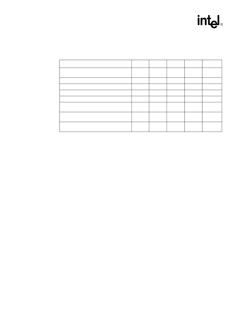
Table 25. Stop Grant/Sleep/Deep Sleep/Enhanced Intel SpeedStep Technology AC
Specifications
T# Parameter
Min
Max
Unit
Figure
Notes
T70: SLP# Signal Hold Time from Stop Grant
Cycle Completion
100
BCLKs
23
T71: Input Signals Stable to SLP# Assertion
10
BCLKs
23
,
24
1
T72: SLP# to DPSLP# Assertion
10
BCLKs
23
T73: Deep Sleep PLL Lock Latency
0
30
μ
s
23
2
T74: SLP# Hold Time from PLL Lock
0
ns
23
T75: STPCLK# Hold Time from SLP#
Deassertion
10
BCLKs
23
T76: Input Signal Hold Time from SLP#
Deassertion
10
BCLKs
23
,
24
T77: VID[4:0] Output Valid Delay from DPSLP#
Assertion
0
10
μ
s
24
相關(guān)PDF資料 |
PDF描述 |
|---|---|
| RH80532NC021256 | Microprocessor |
| RH80532NC025256 | Microprocessor |
| RH80532NC029256 | Microprocessor |
| RH80532NC033256 | Microprocessor |
| RHE070 | Poly Switch PTC DEVICES |
相關(guān)代理商/技術(shù)參數(shù) |
參數(shù)描述 |
|---|---|
| RH80532NC021256 | 制造商:未知廠家 制造商全稱:未知廠家 功能描述:Microprocessor |
| RH80532NC025256 | 制造商:未知廠家 制造商全稱:未知廠家 功能描述:Microprocessor |
| RH80532NC029256 | 制造商:未知廠家 制造商全稱:未知廠家 功能描述:Microprocessor |
| RH80532NC033256 | 制造商:未知廠家 制造商全稱:未知廠家 功能描述:Microprocessor |
| RH80532NC049256 | 制造商:Rochester Electronics LLC 功能描述:- Bulk |
發(fā)布緊急采購(gòu),3分鐘左右您將得到回復(fù)。