- 您現(xiàn)在的位置:買賣IC網(wǎng) > PDF目錄373275 > RK80532PC041512 Microprocessor PDF資料下載
參數(shù)資料
| 型號: | RK80532PC041512 |
| 英文描述: | Microprocessor |
| 中文描述: | 微處理器 |
| 文件頁數(shù): | 16/86頁 |
| 文件大小: | 882K |
| 代理商: | RK80532PC041512 |
第1頁第2頁第3頁第4頁第5頁第6頁第7頁第8頁第9頁第10頁第11頁第12頁第13頁第14頁第15頁當(dāng)前第16頁第17頁第18頁第19頁第20頁第21頁第22頁第23頁第24頁第25頁第26頁第27頁第28頁第29頁第30頁第31頁第32頁第33頁第34頁第35頁第36頁第37頁第38頁第39頁第40頁第41頁第42頁第43頁第44頁第45頁第46頁第47頁第48頁第49頁第50頁第51頁第52頁第53頁第54頁第55頁第56頁第57頁第58頁第59頁第60頁第61頁第62頁第63頁第64頁第65頁第66頁第67頁第68頁第69頁第70頁第71頁第72頁第73頁第74頁第75頁第76頁第77頁第78頁第79頁第80頁第81頁第82頁第83頁第84頁第85頁第86頁
16
Datasheet
Intel
Pentium
III Processor with 512KB L2 Cache at 1.13GHz to 1.40GHz
2.3
Power and Ground Pins
The operating voltage for the Intel Pentium
III
processor with 512KB L2 Cache is the same for
the core and the L2 cache. V
CCCORE
is defined as the power pins that supply voltage to the
processor’s core and cache. The voltage regulator module (VRM) or voltage regulator is
controlled by the five voltage identification (VID) signals driven by the processor.
signals specify the voltage required by the processor core. Refer to
Section 2.6
for further details
on the VID voltage settings.
The VID
The Intel Pentium
III
processor with 512KB L2 cache has 74 V
CCCORE
, 7 V
REF
, 20 V
TT
,
V
CCCMOS1.5
, V
CCCMOS1.8,
V
CCCMOS2.0
and 74 V
SS
inputs. The V
REF
inputs are used as the AGTL
reference voltage for the processor. The V
TT
inputs (1.25V) are used to provide an AGTL
termination voltage to the processor. V
CCCMOS1.5
and V
CCCMOS1.8
and V
CCCMOS2.0
are not
voltage input pins to the processor but rather voltage sources for the pullup resistors which are
connected to CMOS (non-AGTL) input/output signals driven to/from the processor. The V
SS
inputs are ground pins for the processor core and L2 cache.
On the platform, all V
CCCORE
pins must be connected to a voltage island (an island is a portion of
a power plane that has been divided, or an entire plane) to minimize any voltage drop that may
occur due to trace impedance. It is also highly recommended for the platform to provide either a
voltage island or a wide trace for the V
TT
pins. Similarly, all Vss pins must be connected to a
system ground plane. These recommendations can be found in the platform design guide layout
section.
2.3.1
Phase Lock Loop (PLL) Power
It is highly critical that phase lock loop power delivery to the processor meets Intel’s requirements.
A low pass filter is required for power delivery to pins PLL1 and PLL2. This serves as an isolated,
decoupled power source for the internal PLL. Please refer to the Phase Lock Loop Power section in
the appropriate platform design guide for the recommended filter implementation.
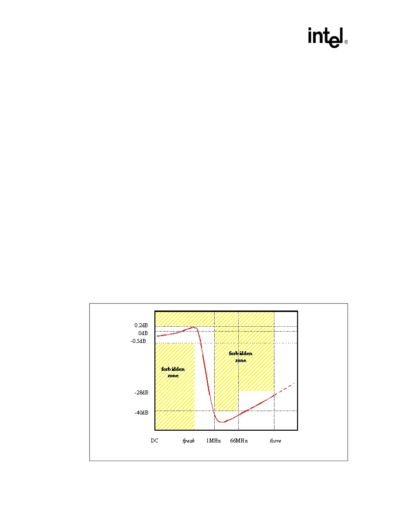
Figure 4. PLL Filter Specification
相關(guān)PDF資料 |
PDF描述 |
|---|---|
| RK9410 | TRANSISTOR | MOSFET | N-CHANNEL | 30V V(BR)DSS | 7A I(D) | SO |
| RKC-SERIES | Interface IC |
| RKCB-SERIES | Interface IC |
| RKCR-SERIES | Interface IC |
| RKCS-SERIES | Interface IC |
相關(guān)代理商/技術(shù)參數(shù) |
參數(shù)描述 |
|---|---|
| RK80532PC041512 SL5YR | 制造商:Intel 功能描述: |
| RK80532PC041512S L66R | 制造商:Intel 功能描述:MPU Pentium? 4 Processor 64-Bit 0.13um 2GHz 478-Pin FCPGA2 |
| RK80532PC041512S L6PK | 制造商:Intel 功能描述:MPU Pentium? 4 Processor 64-Bit 0.13um 2GHz 478-Pin FCPGA2 制造商:Intel 功能描述:32BIT MPU 80532PC041512 2G 512 - Trays 制造商:Intel 功能描述:NORTHWOOD; MPU PENTIUM 4 NETBURST 64BIT 0.13UM 2GHZ - Trays |
| RK80532PC041512SL6 | 制造商:Intel 功能描述:ITLRK80532PC041512SL6PK MPU MM#850362 |
| RK80532PC041512SL6PK | 制造商:Intel 功能描述:ITLRK80532PC041512SL6PK MM# 850362 / 32 |
發(fā)布緊急采購,3分鐘左右您將得到回復(fù)。