- 您現(xiàn)在的位置:買(mǎi)賣(mài)IC網(wǎng) > PDF目錄192305 > S71GL064A08BAI0F3 (SPANSION LLC) Stacked Multi-Chip Product (MCP) Flash Memory and RAM PDF資料下載
參數(shù)資料
| 型號(hào): | S71GL064A08BAI0F3 |
| 廠商: | SPANSION LLC |
| 元件分類(lèi): | 存儲(chǔ)器 |
| 英文描述: | Stacked Multi-Chip Product (MCP) Flash Memory and RAM |
| 中文描述: | SPECIALTY MEMORY CIRCUIT, PBGA56 |
| 封裝: | 7 X 9 MM, 1.20 MM HEIGHT, LEAD FREE, FBGA-56 |
| 文件頁(yè)數(shù): | 73/134頁(yè) |
| 文件大?。?/td> | 2383K |
| 代理商: | S71GL064A08BAI0F3 |
第1頁(yè)第2頁(yè)第3頁(yè)第4頁(yè)第5頁(yè)第6頁(yè)第7頁(yè)第8頁(yè)第9頁(yè)第10頁(yè)第11頁(yè)第12頁(yè)第13頁(yè)第14頁(yè)第15頁(yè)第16頁(yè)第17頁(yè)第18頁(yè)第19頁(yè)第20頁(yè)第21頁(yè)第22頁(yè)第23頁(yè)第24頁(yè)第25頁(yè)第26頁(yè)第27頁(yè)第28頁(yè)第29頁(yè)第30頁(yè)第31頁(yè)第32頁(yè)第33頁(yè)第34頁(yè)第35頁(yè)第36頁(yè)第37頁(yè)第38頁(yè)第39頁(yè)第40頁(yè)第41頁(yè)第42頁(yè)第43頁(yè)第44頁(yè)第45頁(yè)第46頁(yè)第47頁(yè)第48頁(yè)第49頁(yè)第50頁(yè)第51頁(yè)第52頁(yè)第53頁(yè)第54頁(yè)第55頁(yè)第56頁(yè)第57頁(yè)第58頁(yè)第59頁(yè)第60頁(yè)第61頁(yè)第62頁(yè)第63頁(yè)第64頁(yè)第65頁(yè)第66頁(yè)第67頁(yè)第68頁(yè)第69頁(yè)第70頁(yè)第71頁(yè)第72頁(yè)當(dāng)前第73頁(yè)第74頁(yè)第75頁(yè)第76頁(yè)第77頁(yè)第78頁(yè)第79頁(yè)第80頁(yè)第81頁(yè)第82頁(yè)第83頁(yè)第84頁(yè)第85頁(yè)第86頁(yè)第87頁(yè)第88頁(yè)第89頁(yè)第90頁(yè)第91頁(yè)第92頁(yè)第93頁(yè)第94頁(yè)第95頁(yè)第96頁(yè)第97頁(yè)第98頁(yè)第99頁(yè)第100頁(yè)第101頁(yè)第102頁(yè)第103頁(yè)第104頁(yè)第105頁(yè)第106頁(yè)第107頁(yè)第108頁(yè)第109頁(yè)第110頁(yè)第111頁(yè)第112頁(yè)第113頁(yè)第114頁(yè)第115頁(yè)第116頁(yè)第117頁(yè)第118頁(yè)第119頁(yè)第120頁(yè)第121頁(yè)第122頁(yè)第123頁(yè)第124頁(yè)第125頁(yè)第126頁(yè)第127頁(yè)第128頁(yè)第129頁(yè)第130頁(yè)第131頁(yè)第132頁(yè)第133頁(yè)第134頁(yè)
February 8, 2005 S71GL064A_00_A2
S71GL064A based MCPs
41
Advance
Informatio n
Autoselect Command Sequence
The autoselect command sequence allows the host system to read several identifier codes at
specific addresses:
Note: The device ID is read over three cycles. SA = Sector Address
The autoselect command sequence is initiated by first writing two unlock cycles. This is fol-
lowed by a third write cycle that contains the autoselect command. The device then enters
the autoselect mode. The system may read at any address any number of times without ini-
tiating another autoselect command sequence:
The system must write the reset command to return to the read mode (or erase-suspend-
read mode if the device was previously in Erase Suspend).
Enter Secured Silicon Sector/Exit Secured Silicon
Sector Command Sequence
The Secured Silicon Sector region provides a secured data area containing an 8-word/16-byte
random Electronic Serial Number (ESN). The system can access the Secured Silicon Sector
region by issuing the three-cycle Enter Secured Silicon Sector command sequence. The de-
vice continues to access the Secured Silicon Sector region until the system issues the four-
cycle Exit Secured Silicon Sector command sequence. The Exit Secured Silicon Sector com-
mand sequence returns the device to normal operation. Table 10 shows the address and data
requirements for both command sequences. See also “Secured Silicon Sector Flash
Memory Region” for further information. Note that the ACC function and unlock bypass modes
are not available when the Secured Silicon Sector is enabled.
Word Program Command Sequence
Programming is a four-bus-cycle operation. The program command sequence is initiated by
writing two unlock write cycles, followed by the program set-up command. The program ad-
dress and data are written next, which in turn initiate the Embedded Program algorithm. The
system is not required to provide further controls or timings. The device automatically pro-
vides internally generated program pulses and verifies the programmed cell margin. Tables
31 and 32 show the address and data requirements for the word program command se-
quence, respectively.
When the Embedded Program algorithm is complete, the device then returns to the read
mode and addresses are no longer latched. The system can determine the status of the pro-
gram operation by using DQ7 or DQ6. Refer to the Write Operation Status section for
information on these status bits. Any commands written to the device during the Embedded
Program Algorithm are ignored. Note that the Secured Silicon Sector, autoselect, and CFI
functions are unavailable when a program operation is in progress. Note that a hardware
reset immediately terminates the program operation. The program command sequence
should be reinitiated once the device has returned to the read mode, to ensure data integrity.
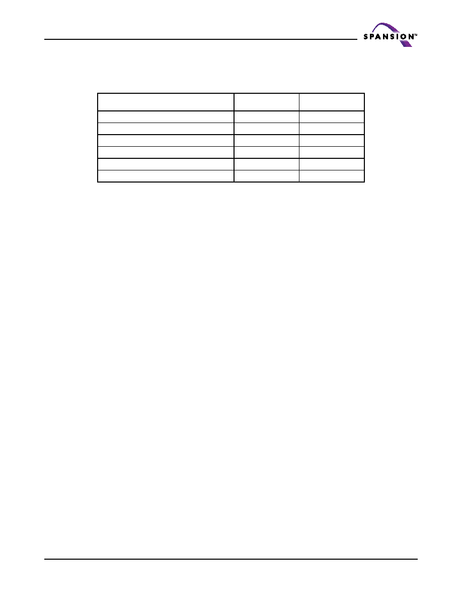
Identifier Code
A7:A0
(x16)
A6:A-1
(x8)
Manufacturer ID
00h
Device ID, Cycle 1
01h
02h
Device ID, Cycle 2
0Eh
1Ch
Device ID, Cycle 3
0Fh
1Eh
Secured Silicon Sector Factory Protect
03h
06h
Sector Protect Verify
(SA)02h
(SA)04h
相關(guān)PDF資料 |
PDF描述 |
|---|---|
| S71GL064A08BAW0B3 | Stacked Multi-Chip Product (MCP) Flash Memory and RAM |
| S71GL064A08BAW0F3 | Stacked Multi-Chip Product (MCP) Flash Memory and RAM |
| S71GL064A08BFI0B2 | Stacked Multi-Chip Product (MCP) Flash Memory and RAM |
| S71GL064A08BFI0B3 | Stacked Multi-Chip Product (MCP) Flash Memory and RAM |
| S71GL064A08BFI0F3 | Stacked Multi-Chip Product (MCP) Flash Memory and RAM |
相關(guān)代理商/技術(shù)參數(shù) |
參數(shù)描述 |
|---|---|
| S71GL064A08BAW0B0 | 制造商:SPANSION 制造商全稱(chēng):SPANSION 功能描述:Stacked Multi-Chip Product (MCP) Flash Memory and RAM |
| S71GL064A08BAW0B2 | 制造商:SPANSION 制造商全稱(chēng):SPANSION 功能描述:Stacked Multi-Chip Product (MCP) Flash Memory and RAM |
| S71GL064A08BAW0B3 | 制造商:SPANSION 制造商全稱(chēng):SPANSION 功能描述:Stacked Multi-Chip Product (MCP) Flash Memory and RAM |
| S71GL064A08BAW0F0 | 制造商:SPANSION 制造商全稱(chēng):SPANSION 功能描述:Stacked Multi-Chip Product (MCP) Flash Memory and RAM |
| S71GL064A08BAW0F2 | 制造商:SPANSION 制造商全稱(chēng):SPANSION 功能描述:Stacked Multi-Chip Product (MCP) Flash Memory and RAM |
發(fā)布緊急采購(gòu),3分鐘左右您將得到回復(fù)。