- 您現(xiàn)在的位置:買賣IC網(wǎng) > PDF目錄16381 > SI3000SSI-EVB (Silicon Laboratories Inc)BOARD EVAL PARALLEL PORT SI3000 PDF資料下載
參數(shù)資料
| 型號: | SI3000SSI-EVB |
| 廠商: | Silicon Laboratories Inc |
| 文件頁數(shù): | 33/34頁 |
| 文件大小: | 0K |
| 描述: | BOARD EVAL PARALLEL PORT SI3000 |
| 標準包裝: | 1 |
| 主要目的: | 音頻編解碼器 |
| 已用 IC / 零件: | SI3000 |
| 已供物品: | 主板和子卡組套 |
第1頁第2頁第3頁第4頁第5頁第6頁第7頁第8頁第9頁第10頁第11頁第12頁第13頁第14頁第15頁第16頁第17頁第18頁第19頁第20頁第21頁第22頁第23頁第24頁第25頁第26頁第27頁第28頁第29頁第30頁第31頁第32頁當前第33頁第34頁
Si3000
8
Rev. 1.4
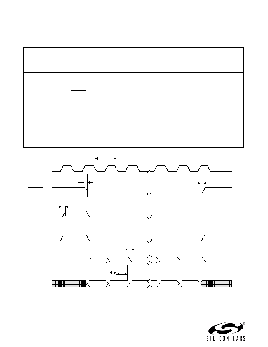
Figure 2. Serial Interface Timing Diagram
Table 7. Switching Characteristics—Serial Interface
(VA, VD = 5 V ±5% or 3.3 V ±10%, TA = 0 to 70°C, CL = 20 pF)
Parameter
Symbol
Test Condition
Min
Typ
Max
Unit
Cycle Time, SCLK
tc
354
1/256 Fs
—
ns
SCLK Duty Cycle
tdty
—
50
—
%
Delay Time, SCLK
to FSYNC
td1
—
10
ns
Delay Time, SCLK
to SDO Valid
td2
—
20
ns
Delay Time, SCLK
to FSYNC
td3
—
10
ns
Setup Time, SDI, before SCLK
tsu
25
—
ns
Hold Time, SDI, after SCLK
th
20
—
ns
Setup Time, FSYNC (mode 2) before
MCLK
tsu
25
—
ns
Hold Time, FSYNC (mode 2) after
MCLK
th
20
—
ns
Note:
All timing is referenced to the 50% level of the waveform. Input test levels are VIH = VD – 0.4 V, VIL = 0.4 V
SCLK
td1
VOH
VOL
FSYNC
(mode 0)
FSYNC
(mode 1)
td3
16 Bit
SDO
16 Bit
SDI
D0
D1
tsu
th
td2
FSYNC
(mode 2)
D0
... D2
High-Z
D15
D14
D1
D0
D15
D14
tc
相關PDF資料 |
PDF描述 |
|---|---|
| ISL88001/2/3EVAL1Z | EVAL BOARD 1 FOR ISL88001/2/3 |
| M3BBA-2060K | IDC CABLE - MSR20A/MC20F/MSR20A |
| ECM25DRMI | CONN EDGECARD 50POS .156 SQ WW |
| VE-B1P-EY-S | CONVERTER MOD DC/DC 13.8V 50W |
| 6374613-8 | C/A LC-SC DUP 50/125 MM 8M |
相關代理商/技術參數(shù) |
參數(shù)描述 |
|---|---|
| SI-3000V | 制造商:SANKEN 制造商全稱:Sanken electric 功能描述:3-Terminal, Low Dropout Voltage Dropper Type |
| SI3000-X-FS | 制造商:Silicon Laboratories Inc 功能描述:VOICE CODEC W/INTEGRATED MICRO LEADFREE - Rail/Tube |
| SI-3000ZD | 制造商:SANKEN 制造商全稱:Sanken electric 功能描述:Surface-Mount Low Dropout Voltage Linear Regulator ICs |
| SI-3000ZD_11 | 制造商:SANKEN 制造商全稱:Sanken electric 功能描述:Surface-Mount, Low Dropout Voltage |
| SI-3000ZF | 制造商:SANKEN 制造商全稱:Sanken electric 功能描述:5-Terminal, Low Dropout Voltage |
發(fā)布緊急采購,3分鐘左右您將得到回復。